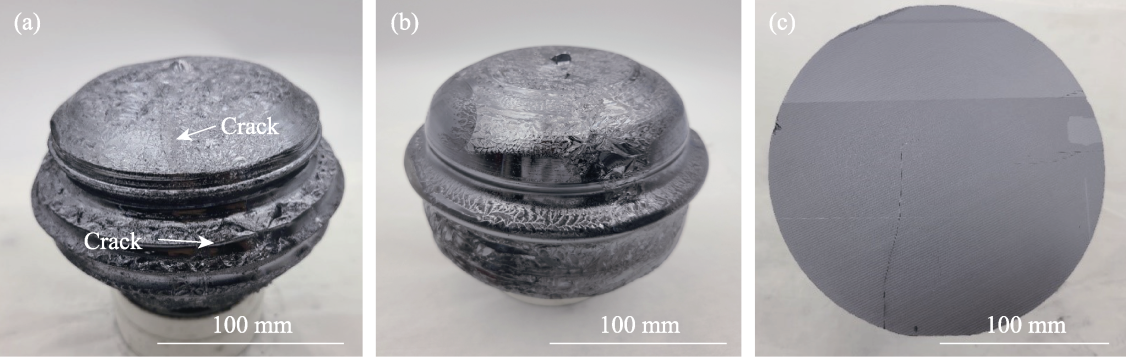
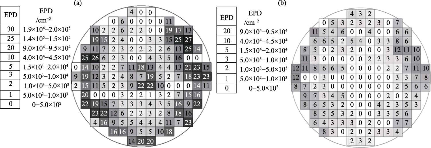
| [1] |
HAMADA H, TSUTSUMI T, SUGIYAMA H, et al. Millimeter- wave InP Device technologies for ultra-high speed wireless communications toward beyond 5G. Proceedings of IEEE International Electron Devices Meeting (IEDM), San Francisco, 2019.
|
| [2] |
AJAYAN J, NIRMAL D. A review of InP/InAlAs/InGaAs based transistors for high frequency applications. Superlattices and Microstructures, 2015, 86: 1.
DOI
URL
|
| [3] |
FANG Y Q, CHEN W, AOT H, et al. InGaAs/InP single-photon detectors with 60% detection efficiency at 1550 nm. Review of Scientific Instruments, 2020, 91(8): 083102.
DOI
URL
|
| [4] |
WANG S. Recent research progress of THz InP HEMT and HBT technologies. Micronanoelectronic Technology, 2018, 55(6): 381.
|
| [5] |
MOUTANABBIR O, GOSELE U. Heterogeneous integration of compound semiconductors. Annual Review of Materials Research, 2010, 40: 469.
DOI
URL
|
| [6] |
MONBERG E M, GAULT W A, DOMINGUEZ F. The growth and characterization of large size, high quality, InP single crystals. Journal of the Electrochemical Society, 1988, 135(2): 500.
DOI
|
| [7] |
JORDAN A S, VONNEIDA A R, CARUSOTHE R. The theory and practice of dislocation reduction in GaAs and InP. Journal of Crystal Growth, 1984, 70(1): 555.
DOI
URL
|
| [8] |
IWASAKI K, SATO K, AOYAMA K. 6-in diameter InP single crystals grown by the hot-wall LEC method and the mirror wafers. IEEE Transactions on Semiconductor Manufacturing, 2003, 16(3): 360.
DOI
URL
|
| [9] |
SHAO H, SUN N, ZHANG X, et al. High quality 6-inch InP single crystal grown by LEC method. Semiconductor Technology, 2020, 45(8): 617.
|
| [10] |
ODA O, KAINOSHO K, KOHIRO K, et al. Development of high quality InP bulk crystals. Journal of Electronic Materials, 1991, 20(12): 1007.
DOI
URL
|
| [11] |
KOHIRO K, OHTA M, ODA O. Growth of long-length 3 inch diameter Fe-doped InP single crystal. Journal of Crystal Growth, 1996, 158(3): 197.
DOI
URL
|
| [12] |
KOHIRO K, KAINOSHO K, ODA O, et al. Growth of low dislocation density InP single crystals by the phosphorus vapor controlled LEC method. Journal of Electronic Materials, 1991, 20(12): 1013.
DOI
URL
|
| [13] |
HOSOKAWA Y, YABUHARA Y, NAKAI R, et al. Development of 4-inch diameter InP single crystal with low dislocation density using VCZ method. 10th Intern. Conf. on Indium Phosphide and Related Materials, Tsukuba, 1998.
|
| [14] |
NODA A, SUZUKI K, ARAKAWA A, et al. 4-inch InP crystals grown by phosphorous vapor controlled LEC method. 14th Indium Phosphide and Related Materials Conference, Stockholm, 2002.
|
 ), SUN Niefeng2(