无机材料学报 ›› 2025, Vol. 40 ›› Issue (12): 1443-1444.DOI: 10.15541/jim20250241 CSTR: 32189.14.jim20250241
所属专题: 【信息功能】介电、铁电、压电材料(202512); 【信息功能】功能晶体(202512)
• 科技进展 • 上一篇
朱一新1,2( ), 喻志奎1, 万青1()
ZHU Yixin1,2(), YU Zhikui1, WAN Qing1()
1. 大尺寸功能晶圆临时键合与减薄.mp4(28892KB)
摘要:
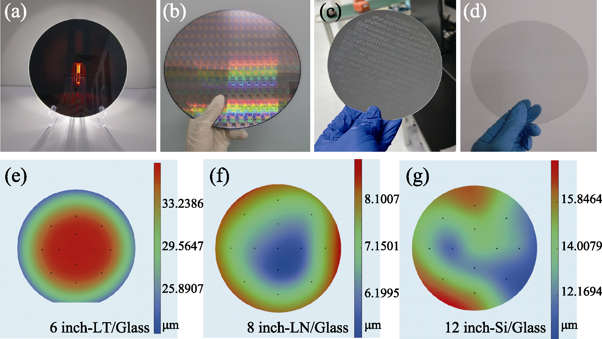
在后摩尔时代, 大尺寸功能晶圆临时键合与超薄减薄技术已成为半导体产业创新的重要支撑。然而, 在晶圆减薄过程中, 翘曲和破损等问题普遍存在, 严重制约了器件性能与良率。针对上述挑战, 本团队研发了一种低成本和室温超平整的临时键合工艺, 有效降低了晶圆翘曲风险, 实现了高平整度和高稳定性的晶圆键合。结合国产减薄设备, 本团队成功实现了多项突破: 将8英寸硅晶圆减薄至8 μm; 将12英寸硅功率芯片减薄至15 μm (总厚度变化TTV≤2 μm); 将8英寸铌酸锂减薄至8~10 μm, 可满足多种压电微机电系统(MEMS)需求。目前, 该技术已成功应用于硅、铌酸锂/钽酸锂、氧化镓、磷化铟等多种晶圆体系的异质集成, 为功率芯片和高性能MEMS器件的国产化进程提供了重要支撑。
中图分类号: