

全无机铯铅卤化钙钛矿CsPbX3(X= Cl, Br, I, 或它们的混合物)纳米晶(NCs)因具有长载流子寿命、强光吸收、低制造成本和带隙可调性等独特的性能, 被广泛用于制备光伏电池、发光二极管、激光器和光电探测器等光电器件。这些器件的快速发展对其性能的要求也相应提高, 例如:延长载流子寿命、延长载流子扩散长度[1⇓-3]和提高缺陷容限[4⇓-6]等, 而研究CsPbX3钙钛矿材料的光生电子-空穴复合行为和光生电子弛豫机制可以为其在发光二极管[7-8]、激光器[9]以及光电探测器[10⇓-12]等领域中的应用提供理论依据。CsPbX3钙钛矿材料的结构和光电特性会受到温度、外加电场和环境气氛以及合成工艺条件等的影响[13⇓-15], 其中, 温度[16]对钙钛矿材料的光电导率、载流子浓度、载流子迁移率、扩散长度、离子传输特性以及它们在光激发后的时间演变[17⇓⇓⇓⇓-22]等方面的影响最为显著。目前在电荷载流子动力学的研究中, 所采取的方法通常是从空间电荷限制电流(Space charge limited current, SCLC)和时间分辨光致发光光谱(Time-resolved photoluminescence, TPRL)中提取光致发光寿命, 然而这些技术不能区分钙钛矿材料中存在的不同缺陷, 也不能评估其缺陷参数[23⇓⇓-26]。而深能级瞬态光谱(Deep level transient spectroscopy, DLTS)和热导纳光谱(Thermal admittance spectroscopy, TAS)则是通过改变电压来区分缺陷态的类型和对缺陷参数进行表征。实际上这些技术涉及制造钙钛矿器件的复杂工艺(包括与钙钛矿层相邻的电荷传输层的工艺), 而制造钙钛矿器件工艺的复杂性阻碍了深能级瞬态光谱和热导纳光谱方法直接用于钙钛矿缺陷的表征[27-28]。
为了更直接地定量表征全无机铯铅卤化钙钛矿的缺陷特性, 光诱导电流瞬态光谱(Photo-induced current transient spectroscopy, PICTS)可以直接用来评估钙钛矿材料缺陷参数[29], 测量光激发后瞬态电压或电流是一种可以提供有关电子浓度、传输和复合信息的方法[30]。本研究采用一种更简便直观的瞬态光电导薄膜样品制备方法, 利用自行设计的一套真空光诱导电流瞬态光电导测试系统(PICTS)在不同温度、不同激发光强度下光激发CsPbBr3光电导样品并测量其回复到起始条件的弛豫过程, 研究光生电流随时间变化的数据, 并表征其结构。该研究方法为研究光激发载流子的动力学相关行为提供了一个新思路。
1 实验方法
1.1 实验原料
溴化铯(CsBr, 99.9%)、溴化铅(PbBr2, 99%)、油酸(C18H34O2, AR)、油胺(C8H19N, AR)、N, N-二甲基甲酰胺(C3H7NO, 90%)、乙酸甲酯(C3H6O2, AR)、正己烷(C6H14, AR)和甲苯(C7H8, AR)均购于阿拉丁化学试剂有限公司, 未经纯化直接使用。
1.2 胶体CsPbBr3 NCs的制备
采用Seth等[31]报道的方法合成CsPbBr3纳米晶。在20 mL试剂瓶中, 将0.06 g溴化铯和0.10 g溴化铅溶解在4 mL的N, N-二甲基甲酰胺中, 然后加入60 μL油酸和0.25 mL油胺制得前驱体溶液。在15 mL圆底瓶中, 加入4 mL甲苯, 在剧烈搅拌状态下, 将200 μL的前驱体溶液添加到甲苯溶液中反应5 min。然后加入4 mL乙酸甲酯, 将混合溶液以9000 r/min离心6 min, 离心后丢弃上清液, 将沉淀物用甲苯洗涤、离心机离心, 重复上述操作3次, 得到CsPbBr3纳米晶,分散在正己烷中备用。
1.3 光电导薄膜样品的制备
将厚度为1.1 mm的氟掺杂的SnO2(FTO)导电玻璃切成规格为20 mm×20 mm的小片, 并用乙醇和去离子水洗涤10 min, 在N2气氛中干燥。利用激光在20 mm×20 mm的小片的中心刻蚀出宽度为0.5 mm、长度为20 mm、深度为200 nm的凹槽, 去除该区域的FTO导电膜。随后将激光刻蚀的FTO玻璃在超声清洗机中用洗涤剂、丙酮、乙醇和去离子水超声清洗, 并在N2气氛中干燥。将干燥的FTO玻璃用透明胶带贴在刻蚀凹槽的两侧, 只露出中间被蚀刻的凹槽, 为保证分散在正己烷中的CsPbBr3纳米晶溶液均匀涂覆在FTO玻璃上, 将FTO玻璃以1300 r/min旋涂3 min, 然后撕下透明胶带, 得到只有凹槽上涂覆有CsPbBr3薄膜的样品, 为了使CsPbBr3纳米晶和FTO玻璃接触良好并不让CsPbBr3晶体结构发生不可逆的变化(温度超过130 ℃时CsPbBr3纳米晶将发生不可逆结构变化), 将样品置于100 ℃氮气氛中退火1 h, 得到CsPbBr3薄膜光电导样品。光电导薄膜样品的制备流程和瞬态光电导测试原理, 如图1所示。
图1
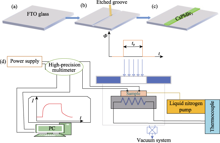
图1
CsPbBr3 NC薄膜样品的制备流程和瞬态光电导测试原理
Fig. 1
Preparation process of CsPbBr3 NC thin film sample and schematic diagram of the transient photoconduction test
(a-c) Preparation process of photoconductive samples; (d) Schematic diagram of the transient photoconduction test
1.4 样品表征
使用UV2600紫外-可见分光光度计(日本Shimadzu)测量分散在正己烷中的CsPbBr3 NCS溶液的光吸收。使用荧光分光光度计(TM/QM/NIR, PTI)测试分散在己烷中的CsPbBr3 NCS溶液的光致发光光谱。利用德国布鲁克AXS公司的 D8 Advance X射线衍射仪进行物相分析。利用日本电子公司型号为 JEM-2100F场发射高分辨率透射电子显微镜表征纳米颗粒的尺寸、形貌和分布。
本实验所用的真空瞬态光电导测试系统是在Gordillo等[32]报道的瞬态光电导测试电路原理的基础上, 结合实际测量的需求, 自行设计了一套真空光诱导电流瞬态光电导测试系统(PICTS)。该系统由源测量单元(Keithley 2450)、数字万用表(Keithley DMM 7510)、四探针样品台(Instec)和温度控制器等组成。温度控制器(Instec MK 2000)通过热电偶加热和液氮泵及水循环泵(Instec LN2P)的运行控制样品温度。样品测量室的真空度由连接到样品室的真空泵(VACUUM -Air-TC110 Pfeiffer)控制, 电离真空规(ZDK-3LED Chengdu Zhenghua)测量真空度。激发光的发光强度由配备有UV检测器(Newport 818-UV)的光功率计(Newport 843-R)检测记录。
在改进的真空瞬态光电导测试系统当中, 采用双探针直接与FTO玻璃导电层接触组成测试电路, 测试样品的光激发瞬态电流。这与传统的模式相比减少了钙钛矿器件中的复杂工艺影响(包括与钙钛矿层相邻的电荷传输层中的工艺), 更能直接反映CsPbBr3纳米晶薄膜的相关特性。在所有测试中, 源测量单元(Keithley 2450)输出的电压和数字万用表(Keithley DMM 7510)测试的光生电流以及激光器单色光脉冲光照周期都由计算机安装的Kickstart 2.7软件(Tektronix)控制和记录数据。单模光纤激光器(450 nm)用作激发光源, 利用任意波形函数发生器AFG 1062(Tektronix)控制激发光源和数字万用表(Keithley DMM 7510), 并调节相应的频率和相位, 以实现测试目的。
在脉冲激光辐照和固定电压下监测CsPbBr3光电导器件中的光生电流瞬态变化。通过激光器输出持续时间tp和光子能量hν>Eg的近单色光脉冲照射样品, 其中Eg是CsPbBr3的能带隙。激发照射时光生电流上升, 固定tp时间长度, 一旦激发光脉冲结束, 光生电流迅速下降。采用0~40 V单向电压扫描样品, 监测恒压光激发的瞬态光生电流, 获得相关测试数据。
2 结果与讨论
2.1 CsPbBr3 NCs的结构和形貌
图2(a~d)分别为CsPbBr3 NCs 在正己烷中的吸收光谱、PL发射光谱和XRD图谱、TEM和HRTEM照片。从图2(a)可以看出, CsPbBr3 NC的吸收带非常宽, 激子吸收峰的波长为497 nm, 这是由NC 的尺寸分布或NC中激子的热电离[33]所引起。CsPbBr3 NCs 在511 nm处有一个PL发射峰, 该PL发射可能源自自由激子的辐射复合或束缚激子。从图2(b) XRD图谱可以看出, 在FTO玻璃上涂覆CsPbBr3薄膜样品在2θ=15.1°、21.5°、26.5°、30.7°、37.8°、43.7°处出现衍射峰, 分别对应于CsPbBr3的(001)、(110)、(¯111)、(200)、(1¯21)、(202)晶面, 与标准CsPbBr3的PDF卡片(JCPDS 18-0364)比对发现, 所制备的CsPbBr3薄膜样品为四方相钙钛矿晶体结构。从图2(c)TEM照片可以看出, CsPbBr3纳米晶呈规则的立方体形貌, 尺寸分布较均匀, 纳米晶分散良好, 晶粒的平均尺寸大小为17 nm。图2(d)高分辨HRTEM照片可以看出, CsPbBr3纳米晶都具有清晰的晶格条纹, 表明制备的样品具有良好的结晶度, 晶格条纹间距均为0.291 nm, 对应CsPbBr3纳米晶的(200)晶面。
图2
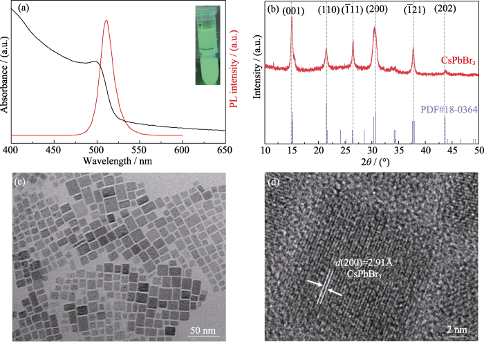
图2
CsPbBr3 NCs的光吸收和PL光谱及其结构与形貌图
Fig. 2
Optical absorption, PL spectra, microstructure and micromorphology of CsPbBr3 NCs
(a) Optical absorption and PL spectra of CsPbBr3 NCs in n-hexane; (b) XRD pattern; (c) TEM image; (d) High resolution TEM image
2.2 CsPbBr3纳米晶在不同温度和不同功率的瞬态光电导
在测试各个温度下的瞬态光电导之前, 需要检测探针与FTO导电玻璃之间的接触状态, 为此测试了不同温度下, 电压在0~40 V范围内变化的归一化电压-电流曲线。从图3(a)可以看出电压在0~40 V范围内, 随着电压升高电流不断增大, 各个曲线并不存在整流区间, 说明在各温度下FTO薄膜与探针之间不存在接触势垒, 为欧姆接触。由于在不同温度下CsPbBr3的能带隙稍有差异, 使得在各温度下随着电压的升高, 电流增长速度各不相同。
图3
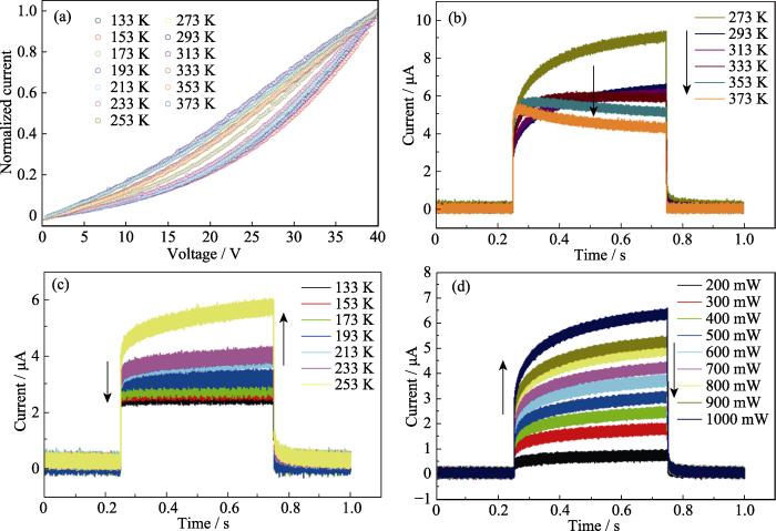
图3
在不同温度和激发功率下光电导样品的光生电流随光循环时间(t)的变化曲线
Fig. 3
Curves of photo-generated current with light cycle time(t) at different temperatures and excitation powers for photoconductive samples
(a) Current-voltage curve of 0-40 V measured at 133-373 K; (b, c) Curves of photo-generated current change with light cycle time at different temperatures; (d) Curves of photo-generated current change with light cycle time at different laser excitation power; Colorful figures are available on website
从图3(b, c)可知, 当温度在133~313 K区间时, 各个温度的光生电流-时间曲线非常相似, 开灯状态时光生电流先迅速上升, 在随后0.5 s的开灯时间里光生电流一直缓慢增加, 直到关灯时光生电流快速下降。但是在333~373 K温度范围内, 随着温度的升高, 曲线的形状出现了较大变化, 具体原因将在2.3节讨论。
2.3 温度相关载流子动力学的瞬态光电导
图4
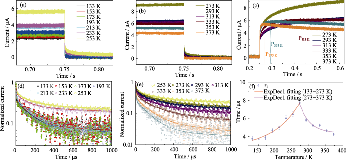
图4
光电导样品的温度相关的载流子光生电流和最快衰减时间常数曲线
Fig. 4
Curves of temperature-dependent carrier photo-generated currents and the fastest decay time constants of the photoconductive samples
Enlarged views of (a, b) falling and (c) rising edges with temperature changed from 133 to 373 K; (d, e) Normalized current-time curves and their fitting curves of temperature changed with temperature; (f) The fastest decay time constant τ1 obtained by fitting from experimental data of (d, e) with temperature change; Colorful figures are available on website
光诱导电流瞬态光谱表征需要载流子产生及复合的动力学过程信息, 即:载流子浓度随时间变化的趋势。瞬态光电流大小反映了载流子浓度的高低, 为此, 在微秒级的时间窗口内, 绘制了133~373 K范围从激光关闭往后1000 μs的归一化光生电流-时间变化图(如图4(d, e)的点图)。
为了描述多种载流子光激发载流子的动力学过程, 一般半导体薄膜的瞬态光电导动力学可以用多指数项的和来描述。考虑到本实验中所用光源的激发功率较高, 所以用曲线拟合程度较好的三指数衰减函数拟合:每一个温度(T)下的光生电流强度ΔI随时间(t)变化曲线用公式(1)进行三指数项的和进行拟合[36]:
其中,A、B和C是拟合参数, τ1、τ2和τ3为三指数拟合的各种载流子衰减时间常数。当载流子寿命在皮秒到纳秒尺度时, 陷阱辅助复合、二阶复合和俄歇复合均存在。而在微秒尺度下, 各类载流子的产生和复合在皮秒至纳秒尺度下皆达到了动态平衡, 在迁移率不发生变化的情况下, 净单激发载流子则为使光生电流升高的净载流子。此时净载流子与晶格中的声子主导了一阶衰减项(A(T)e−t/τ1), 而二阶衰减项除了考虑载流子与晶格中的声子的相互作用外, 还需考虑离子迁移等其他因素与载流子、晶格中的声子的相互作用, 二阶衰减项为:B(T)e−t/τ1-A(T)e−t/τ2。三阶衰减项还要考虑陷阱态的相关作用。本实验拟合得到的在不同温度下归一化光生电流-时间曲线的衰减时间常数τ1、τ2以及τ3, 如表1所示, 并分析了τ1的变化规律。三指数拟合曲线为图4 (d, e)中的实线部分, 拟合的最快衰减时间常数τ1绘制在图4(f)中。分析实验结果发现温度为273 K时有着比其他温度更大的τ1, 在273 K左侧低温度的区间, 随着温度升高, τ1增大。在273 K右侧的高温区间, τ1则是随着温度升高, 逐渐减小, 两个区间的τ1随温度变化趋势都能用单指数函数很好地拟合。实验结果表明在273 K附近(这个温度可能跟材料的晶粒大小以及不同陷阱状态等因素有关)CsPbBr3纳米晶体有着比其他温度更慢的载流子弛豫速率。
表1 不同温度下时间-归一化光生电流曲线的各拟合参数
Table 1
| Temperatures/K | τ1/μs | τ2/μs | τ3/μs |
|---|---|---|---|
| 133 | (3.759±0.223) | (124.77±6.69) | (1324.35±361.18) |
| 153 | (3.723±0.216) | (127.40±5.72) | (1545.52±582.47) |
| 173 | (3.885±0.209) | (134.73±6.23) | (2141.44±1403.33) |
| 193 | (4.680±0.260) | (107.52±5.69) | (720.84±118.71) |
| 213 | (5.015±0.240) | (128.03±4.42) | (1473.34±412.23) |
| 233 | (5.985±0.322) | (124.42±4.29) | (1725.43±171.92) |
| 253 | (6.439±0.270) | (133.90±3.88) | (1535.70±80.51) |
| 273 | (7.721±0.193) | (133.68±2.92) | (1249.10±30.38) |
| 293 | (5.792±0.152) | (121.84±2.33) | (1249.65±34.02) |
| 313 | (5.176±0.140) | (123.42±2.59) | (1215.50±43.39) |
| 333 | (5.238±0.137) | (119.48±2.78) | (1061.38±47.03) |
| 353 | (4.638±0.114) | (115.78±3.05) | (1127.95±113.98) |
| 373 | (4.254±0.128) | (116.16±4.02) | (2370.56±1223.21) |
一般来说仅仅温度发生改变而其他因素不发生改变时, 光电导样品的瞬时光生电流大小与瞬时载流子浓度成正相关。从温度133 K开始, 当温度开始上升时, 更多低能级的电子可以被激发。这导致了载流子浓度增加, 反映在图4(a, b)的瞬时光生电流开始增大, 从而提高了载流子弛豫速率, 但是温度升高时, 晶格振动开始足以容纳丰富的高频模式即LO 模式[16,37⇓-39], 这就导致了载流子-LO声子相互作用更加强烈, 从而整体上降低了载流子弛豫速率, 这表现为在133~273 K范围, 随着温度升高, τ1增大。载流子浓度和载流子-声子之间的相互作用都影响弛豫速率, 但是要确定一个具体的关系式非常复杂。当温度升高到273 K以上时, 即使载流子-声子相互作用变得更强烈了, 随着温度从273 K升高到373 K, 载流子浓度也随之减小, 反映在图4(a, b)的瞬时光生电流大小开始减少, 虽然载流子弛豫速率受到载流子-声子耦合的影响, 但是此时载流子浓度对τ1影响更大, 表现为在273~373 K区间τ1随着温度升高而减小。
2.4 激发功率相关载流子动力学的瞬态光电导
图5
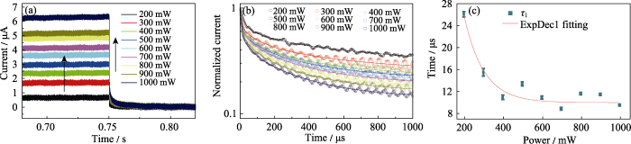
图5
激发功率相关的光电导样品载流子光生电流和最快衰减时间常数曲线
Fig. 5
Curves of excitation power-dependent carrier photo-generated current and the fastest decay time constant of the photoconductive samples
(a) Curve of photo-generated current of samples with light cycle time at different excitation power; (b) Normalized current-time curve and their fitting curve with different excitation power; (c) The fastest decay time constant τ1 obtained by fitting from experimental data of (b) with excitation power change; Colorful figures are available on website
表2 不同功率下时间-归一化光生电流曲线的各拟合参数
Table 2
| Power/mW | τ1/μs | τ2/μs | τ3/μs |
|---|---|---|---|
| 200 | (25.955±0.493) | (117.67±22.31) | (822.18±234.43) |
| 300 | (15.411±0.686) | (91.76±17.61) | (502.61±110.28) |
| 400 | (10.856±0.392) | (86.72±13.96) | (423.04±60.38) |
| 500 | (13.300±0.351) | (100.49±15.70) | (444.26±71.77) |
| 600 | (10.824±0.281) | (52.30±4.84) | (318.36±12.73) |
| 700 | (8.775±0.322) | (74.87±6.95) | (353.29±21.81) |
| 800 | (11.546±0.210) | (62.75±6.64) | (325.15±15.40) |
| 900 | (11.412±0.183) | (89.94±7.53) | (386.28±29.85) |
| 1000 | (9.431±0.132) | (51.78±2.85) | (294.00±7.33) |
3 结论
基于瞬态光电导测试不同温度和不同激发功率条件下光激发CsPbBr3的光生电流-时间曲线, 并详细分析了温度变化和激发功率变化时三指数拟合得到的最快衰减时间常数τ1的变化趋势, 实验结果表明在133~273 K温度范围, τ1随着温度升高而增大; 在273~373 K温度范围,τ1随着温度升高而减小。随着激发功率提高, 光生电流增大, 衰减时间常数τ1减小。这是由于载流子-声子耦合可能在CsPbBr3的光生载流子复合和弛豫过程中起着重要作用, 这为进一步研究基于卤化物钙钛矿半导体的高效太阳能电池和其他光电器件提供了一个新思路, 但仍然需要做更多的工作来全面理解卤化物钙钛矿的载流子弛豫过程。
参考文献
Charge-carrier dynamics in organic-inorganic metal halide perovskites
Band filling with free charge carriers in organometal halide perovskites
High charge carrier mobilities and lifetimes in organolead trihalide perovskites
Low trap-state density and long carrier diffusion in organolead trihalide perovskite single crystals

\n The performance of organic-inorganic hybrid perovskite planar solar cells has steadily improved. One outstanding issue is that grain boundaries and defects in polycrystalline films degrade their output. Now, two studies report the growth of millimeter-scale single crystals. Nie\n et al.\n grew continuous, pinhole-free, thin iodochloride films with a hot-casting technique and report device efficiencies of 18%. Shi\n et al.\n used antisolvent vapor-assisted crystallization to grow millimeter-scale bromide and iodide cubic crystals with charge-carrier diffusion lengths exceeding 10 mm.\n
Spatial and temporal imaging of long-range charge transport in perovskite thin films by ultrafast microscopy
Charge carrier diffusion coefficient and length are important physical parameters for semiconducting materials. Long-range carrier diffusion in perovskite thin films has led to remarkable solar cell efficiencies; however, spatial and temporal mechanisms of charge transport remain unclear. Here we present a direct measurement of carrier transport in space and in time by mapping carrier density with simultaneous ultrafast time resolution and ∼50-nm spatial precision in perovskite thin films using transient absorption microscopy. These results directly visualize long-range carrier transport of ∼220 nm in 2 ns for solution-processed polycrystalline CH3NH3PbI3 thin films. Variations of the carrier diffusion coefficient at the μm length scale have been observed with values ranging between 0.05 and 0.08 cm2 s−1. The spatially and temporally resolved measurements reported here underscore the importance of the local morphology and establish an important first step towards discerning the underlying transport properties of perovskite materials.
Imaging the long transport lengths of photo-generated carriers in oriented perovskite films
Perovskite light-emitting diodes based on solution-processed self-organized multiple quantum wells
Bright light- emitting diodes based on organometal halide perovskite
Low-temperature solution-processed wavelength-tunable perovskites for lasing
High-performance flexible broadband photodetector based on organolead halide perovskite
Large-area perovskite nanowire arrays fabricated by large-scale roll-to-roll micro-gravure printing and doctor blading
High-performance flexible photodetectors based on high-quality perovskite thin films by a vapor-solution method
Zero- dimensional cesium lead halide perovskites: phase transformations, hybrid structures, and applications
In situ observation of a photodegradation-induced blueshift in perovskite nanocrystals using single-particle spectroscopy combined with atomic force microscopy
Ferroelastic domains enhanced the photoelectric response in a CsPbBr3 single-crystal film detector
Temperature-dependent interplay of polaron formation and hot carrier cooling dynamics in CsPbBr3 nanocrystals: role of carrier-phonon coupling strength
Ionic transport in hybrid lead iodide perovskite solar cells
Solar cells based on organic–inorganic halide perovskites have recently shown rapidly rising power conversion efficiencies, but exhibit unusual behaviour such as current–voltage hysteresis and a low-frequency giant dielectric response. Ionic transport has been suggested to be an important factor contributing to these effects; however, the chemical origin of this transport and the mobile species are unclear. Here, the activation energies for ionic migration in methylammonium lead iodide (CH3NH3PbI3) are derived from first principles, and are compared with kinetic data extracted from the current–voltage response of a perovskite-based solar cell. We identify the microscopic transport mechanisms, and find facile vacancy-assisted migration of iodide ions with an activation energy of 0.6 eV, in good agreement with the kinetic measurements. The results of this combined computational and experimental study suggest that hybrid halide perovskites are mixed ionic–electronic conductors, a finding that has major implications for solar cell device architectures.
Direct measurement of the exciton binding energy and effective masses for charge carriers in organic-inorganic tri-halide perovskites
Multifaceted excited state of CH3NH3PbI3. Charge separation, recombination, and trapping
Comparison of recombination dynamics in CH3NH3PbBr3 and CH3NH3PbI3 perovskite films: influence of exciton binding energy
Unraveling charge carriers generation, diffusion, and recombination in formamidinium lead triiodide perovskite polycrystalline thin film
Hot carrier relaxation in CsPbBr3-based perovskites: a polaron perspective
Methylammonium bismuth iodide as a lead-free, stable hybrid organic-inorganic solar absorber
Colloidal synthesis and photophysics of M3Sb2I9 (M=Cs and Rb) nanocrystals: lead-free perovskites
Optoelectronic and photovoltaic properties of the air-stable organohalide semiconductor (CH3NH3)3Bi2I9
Dimensionality controlling of Cs3Sb2I9 for efficient all-inorganic planar thin film solar cells by HCl-assisted solution method
Influence of charge transport layers on capacitance measured in halide perovskite solar cells
Utilization of temperature-sweeping capacitive techniques to evaluate band gap defect densities in photovoltaic perovskites
Assessing the impact of defects on lead-free perovskite-inspired photovoltaics via photoinduced current transient spectroscopy
Interpretation of optoelectronic transient and charge extraction measurements in dye-sensitized solar cells
A facile methodology for engineering the morphology of CsPbX3 perovskite nanocrystals under ambient condition
A facile and highly reproducible room temperature, open atmosphere synthesis of cesium lead halide perovskite nanocrystals of six different morphologies is reported just by varying the solvent, ligand and reaction time. Sequential evolution of the quantum dots, nanoplates and nanobars in one medium and nanocubes, nanorods and nanowires in another medium is demonstrated. These perovskite nanoparticles are shown to be of excellent crystalline quality with high fluorescence quantum yield. A mechanism of the formation of nanoparticles of different shapes and sizes is proposed. Considering the key role of morphology in nanotechnology, this simple method of fabrication of a wide range of high quality nanocrystals of different shapes and sizes of all-inorganic lead halide perovskites, whose potential is already demonstrated in light emitting and photovoltaic applications, is likely to help widening the scope and utility of these materials in optoelectronic devices.
A study of trap and recombination centers in MAPbI3 perovskites
Temperature-dependent photoluminescence of inorganic perovskite nanocrystal films
In situ Raman spectroscopic studies of thermal stability of all-inorganic cesium lead halide (CsPbX3, X = Cl, Br, I) perovskite nanocrystals
Ultrafast photogeneration of charged polarons in conjugated polymers
Terahertz conductivity within colloidal CsPbBr3 perovskite nanocrystals: remarkably high carrier mobilities and large diffusion lengths
Quantum dots: CsPbX3 quantum dots for lighting and displays: room-temperature synthesis, photoluminescence superiorities, underlying origins and white light- emitting diodes
Crystal growth of the perovskite semiconductor CsPbBr3: a new material for high-energy radiation detection
Unveiling lasing mechanism in CsPbBr3 microsphere cavities
