

随着人类社会对可再生能源的需求日益增加, 寻找一种绿色环保的能量转换方式也愈发迫在眉睫。自从Seebeck效应[1]、Peltier效应[2]和Thomson效应被发现以来, 热电材料可以实现热能和电能的直接相互转换, 在应对能源危机问题上展现出极大的应用潜力, 引起了广泛关注[3]。热电转换效率取决于材料的无量纲优值
AgBiSe2化合物存在三种晶体结构, 室温时为六方相(空间群P-3m1), 随温度升高分别在460和580 K附近发生两次相转变, 先转变为菱面体相(空间群R-3m), 最终变为立方相(空间群Fm-3m)。六方相结构中两种占位不同的Bi3+导致Ag+空位较多, 电性能较差, 室温下载流子浓度约为~1018 cm-3[14]。由于AgBiSe2在工作温度范围内需要经历两次结构相变, 使其晶格常数和力学性能在相变点处发生骤变, 应用在热电器件中会产生较高的内部热应力, 影响热电器件的稳定性及服役性能[15-16], 因此获得稳定立方相结构的AgBiSe2, 并优化热电性能至关重要。已有报道[17⇓⇓-20]通过在Ag的位置掺杂Nb、In、Ge或者在Se位置掺杂卤素来提高载流子浓度。近年, 重庆大学周小元课题组[21]和刘小村等[22]发现Sb、Sn掺杂可以降低AgBiSe2的相变温度, 使材料在室温下可以保持稳定的立方相结构, Br掺杂的立方相结构的(AgBiSe2)0.7(PbSe)0.3化合物也展现出优异的热电性能[23-24]。
本研究首先选择无铅的IV-VI族化合物SnTe与AgBiSe2进行合金化, 系统研究了引入SnTe对AgBiSe2物相结构和热电性能的影响, 得到了宽温度范围(300~700 K)内具有稳定立方相结构的(AgBiSe2)0.75(SnTe)0.25热电材料。然后在其Ag位通过掺杂Nb元素, 调节载流子浓度, 引入杂质点缺陷, 系统探究Nb掺杂对其热电性能的影响。
1 实验方法
1.1 样品制备
本研究使用真空熔融法结合放电等离子体烧结工艺(Spark Plasma Sintering, SPS)制备组分为(AgBiSe2)1-x (SnTe)x (x=0.10~0.30)和(Ag1-yNbyBiSe2)0.75(SnTe)0.25 (y= 0.01~0.04)两组样品。在氩气手套箱中, 将高纯金属单质Ag粒(99.999%, 国药集团化学试剂有限公司)、Bi粒(99.999%, 国药集团化学试剂有限公司)、Se粒(99.99%, 中诺新材科技有限公司)、Sn粒(99.999%, 国药集团化学试剂有限公司)、Te块(99.999%, 阿拉丁生化科技股份有限公司)、Nb粉(99.99%, 阿法埃莎公司)按照化学计量比称取, 放入外径为13 mm的石英管中, 真空密封, 悬挂在立式熔融炉中, 在6 h内升温至1373 K保温10 h, 随后在3 h内降温到923 K。退火48 h后, 样品随炉冷却至室温。球磨熔融得到的铸锭(转速300 r/min, 1 h), 球磨后过80 µm(200目)筛, 得到的均匀粉体用SPS烧结得到ϕ10 mm×2 mm的圆片, 烧结条件为673 K, 80 MPa, 保温5 min。最后利用金刚石线切割机将样品切割成测试所需的标准尺寸, 用于性能测试和表征。
1.2 材料表征
采用粉末X射线衍射仪(Rigaku D/Max-2550 PC, 丹东浩元仪器有限公司, CuKα)和原位X射线衍射仪(Empyrean, 荷兰帕纳科公司)表征材料的物相结构。采用场发射扫描电子显微镜(TESCAN MAIA 3, 捷克共和国)和高分辨透射电子显微镜(JEOL JEM-F200, 日本, 加速电压200 kV)观察样品的微观形貌。采用电性能测试设备(ZEM-3, ULVAC-RIKO)同时测得样品的电导率和Seebeck系数。采用激光导热仪(LFA 457, Netzsch), 测得样品的热扩散系数D(m2·s–1)。根据公式
2 结果与讨论
2.1 (AgBiSe2)1-x(SnTe)x的物相组成
图1(a)是熔融合成、细化后(AgBiSe2)1–x(SnTe)x粉末的X射线衍射谱图, x=0.10样品的主峰与六方相结构的AgBiSe2 (PDF#74-0842, 空间群P-3m1)一一对应。随着SnTe含量增大, 峰型逐渐发生变化, 从2θ=44°附近的放大图中可以看出双峰逐渐合并, 峰的强度逐渐增加, x=0.25样品的主峰与立方相结构的AgBiSe2 (PDF 89-3673, Fm-3m)一一对应。衍射峰向左发生轻微偏移, 这是因为加入SnTe使样品的晶格常数线性增加, 如图1(b)所示。比较离子半径可以初步确定离子半径较大的Te2–(0.097 nm)占据了离子半径较小的Se2–(0.05 nm)位置, 而Sn2+(0.069 nm)的离子半径远小于Ag+(0.126 nm)、Bi3+(0.103 nm)的离子半径。立方相结构SnSe可以解释离子半径减小, 晶格常数反而增加的现象[25]。其中Sn–Se键合距离约为0.2995 nm, 远大于Ag/Bi–Se键合距离0.2916 nm[26], 说明Sn2+进入到AgBiSe2中, 导致晶格常数呈现逐步增加的变化趋势。立方相(AgBiSe2)1–x(SnTe)x晶体结构如图1(c)所示。图1(d)为样品(AgBiSe2)1–x(SnTe)x的差示扫描热流曲线。随温度升高, x=0.10样品在333 K附近有一个吸热峰, 523 K附近出现较为尖锐的吸热峰, 分别对应六方相转变为菱面体相和菱面体相转变为立方相。与AgBiSe2的相变温度点(580 K)相比较, 引入SnTe使立方相的相变温度点向低温移动。当x
图1
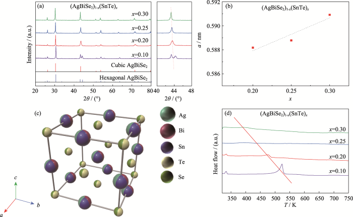
图1
样品(AgBiSe2)1-x(SnTe)x的物相组成
Fig. 1
Phase composition of (AgBiSe2)1-x(SnTe)x samples
(a) XRD patterns of (AgBiSe2)1-x(SnTe)x powder samples at room temperature and their amplification around 2θ=44°; (b) Lattice constant a varied with SnTe content x with the dotted line showing the best linear fitting; (c) Crystal structure of cubic (AgBiSe2)1-x(SnTe)x; (d) Differential scanning calorimeter (DSC) heat flow curves from 300 K to 750 K
2.2 (AgBiSe2)1-x(SnTe)x的热电性能
图2为(AgBiSe2)1-x(SnTe)x样品的热电性能参数随温度的变化关系。如图2(a), 样品的室温电导率随着SnTe含量增大而逐渐降低, 由184 S·cm-1 (x=0.10)降低到55 S·cm-1(x=0.30)。这是由于随着SnTe引入, 过多的空穴载流子中和了AgBiSe2化合物的部分电子[27], 导致室温电导率降低。在300~523 K温度范围内, 随温度升高, x=0.1样品的电导率先升高后降低, 在523 K存在明显的拐点, 对应图1(d)的DSC热流曲线中的相变点; 在523~700 K温度范围内, 随温度升高电导率先升高后降低, 表明相变后立方相AgBiSe2晶体仍表现出半导体传导的特性, 随后电导率出现微弱下降则主要是由于本征激发等原因所导致。随着SnTe含量逐渐增大, AgBiSe2物相结构逐渐变成立方相结构, 电导率在整个测试温度区间呈现平缓升高的趋势, 无明显拐点。图2(b)为(AgBiSe2)1-x(SnTe)x样品的Seebeck系数随温度的变化关系, 图中样品的Seebeck系数为负值, 表明该材料为n型传导特性。随着SnTe含量逐渐增大, 室温Seebeck系数绝对值逐渐增大, 从105.5 μV·K-1增加到185.7 μV·K-1, 表现出与电导率完全相反的变化趋势。x=0.25和0.30样品的Seebeck系数绝对值都呈现先升高后降低的变化趋势, 表现出非简并半导体的特征, 当温度超过400 K时, Seebeck系数绝对值分别从184和196 μV·K-1降低到121和94 μV·K-1, 而这与载流子的本征激发有关[28]。
图2
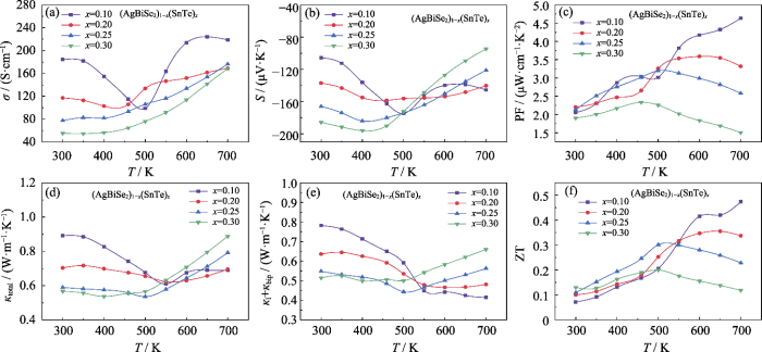
图2
样品(AgBiSe2)1-x(SnTe)x随温度变化的热电性能
Fig. 2
Temperature dependent thermoelectric properties of (AgBiSe2)1-x(SnTe)x samples
(a) Electrical conductivity; (b) Seebeck coefficient; (c) Power factor; (d) Total thermal conductivity; (e) Lattice thermal conductivity; (f) ZT
根据所测的电导率和Seebeck系数, 计算样品的功率因子(Power Factor, PF,
图2(d)为样品总热导率随温度的变化关系, 室温下总热导率随SnTe含量增大逐渐降低, 这是因为引入SnTe使AgBiSe2的晶格逐渐转变为立方相结构, Ag和Bi原子无序化程度增大, 导致化学键非谐性增强, 加剧了声子-声子之间的散射[29], 进一步降低晶格热导率。从图2(e)晶格热导率随温度的变化关系也可以看出, 室温下晶格热导率由六方相的0.76 W·m-1·K-1降低到立方相的0.51 W·m-1·K-1。而x=0.25和0.30样品分别在500和400 K, 热导率开始明显增大。这主要是由于随着温度升高, 样品热传导不再是单一载流子传输, 本征热激发对热导率的贡献增大。图2(f)是样品(AgBiSe2)1-x(SnTe)x的ZT随温度的变化关系, 随着SnTe含量增大, 样品的ZT峰值逐渐降低。对于x=0.25和0.30样品, 由于在500 K左右功率因子降低, 因此相应温度的ZT达到峰值~0.3和~0.2后开始下降。
综上所述, x≥25%时 (AgBiSe2)1-x(SnTe)x样品为立方相结构。而SnTe含量增大会导致其热电性能降低, 因此选择性能较好的立方相结构(AgBiSe2)0.75(SnTe)0.25样品进行后续研究。
2.3 (AgBiSe2)0.75(SnTe)0.25的物相结构分析
AgBiSe2在室温下是六方相结构(空间群P-3m1), 随着温度升高, 分别在460和580 K附近出现两次相变[30]。图3中(AgBiSe2)0.75(SnTe)0.25的XRD谱图在整个测试温度范围内都没有明显变化, 并且也没有相转变过程对应的峰型变化, 图4为高分辨率透射电镜(High Resolution Transmission Electron Microscope, HRTEM)照片以及对应的傅里叶变换(Fast Fourier Transform, FFT)得到的电子衍射图像, 样品分别沿
图3
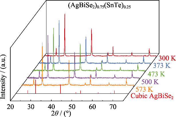
图3
样品(AgBiSe2)0.75(SnTe)0.25与温度相关的XRD谱图
Fig. 3
Temperature dependent XRD patterns of (AgBiSe2)0.75(SnTe)0.25
图4
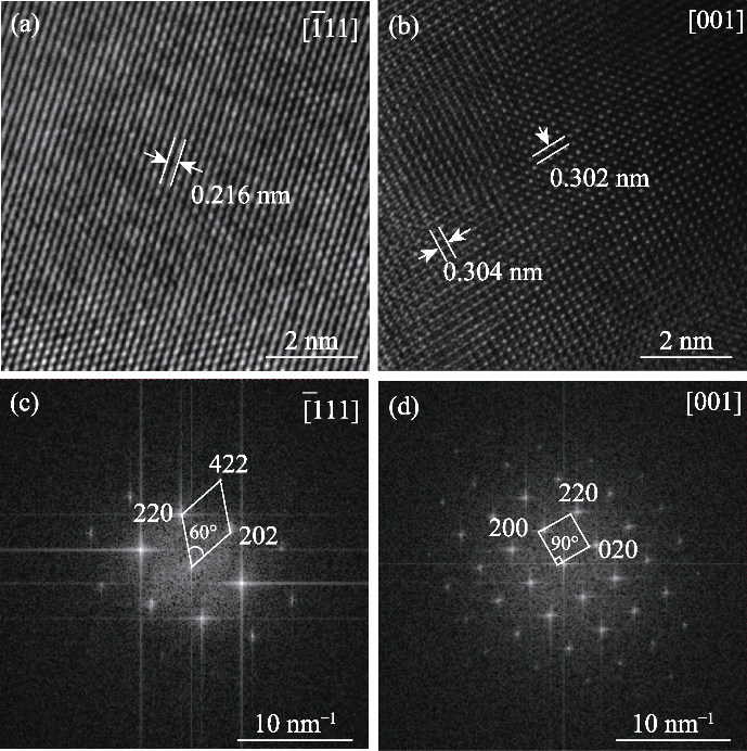
图4
样品(AgBiSe2)0.75(SnTe)0.25沿(a)
Fig. 4
Series HRTEM images along (a)
2.4 Nb掺杂的(Ag1-yNbyBiSe2)0.75(SnTe)0.25化合物
2.4.1 (Ag1-yNbyBiSe2)0.75(SnTe)0.25的物相组成
图5(a)为室温下(Ag1-yNbyBiSe2)0.75(SnTe)0.25样品经过SPS烧结后块体的XRD图谱, 所有样品的XRD峰位都与立方相AgBiSe2(PDF#73-1741, Fm-3m)峰位一一对应。随着Nb掺杂含量逐渐增大, XRD图谱上出现了明显的Nb单质的峰(2θ=38.5°, PDF 89-3715), 说明在(Ag1-yNbyBiSe2)0.75(SnTe)0.25化合物中Nb的固溶极限为0.04左右。由于Nb2+的离子半径(0.064 nm)远小于Ag+的离子半径(0.126 nm), 随着Nb掺杂量增大, 材料的晶格常数逐渐降低, 如图5(b)所示, 当达到固溶极限y=0.04时, 其晶格常数下降更加明显, 主要是由于Nb析出以及Ag+位置空出所导致的。图5(c)为y=0.04样品的面扫描元素分布图, 部分区域Nb元素明显富集, 这也证明化合物中存在Nb单质。
图5
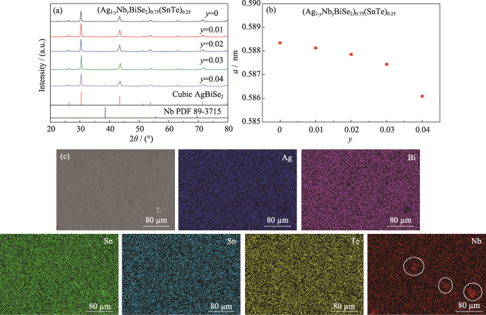
图5
样品(Ag1-yNbyBiSe2)0.75(SnTe)0.25的物相组成
Fig. 5
Phase compositions of (Ag1-yNbyBiSe2)0.75(SnTe)0.25 samples
(a) XRD patterns; (b) Lattice constant a changed with the content of Nb, y for sintered (Ag1-yNbyBiSe2)0.75(SnTe)0.25; (c) Surface scan element distributions of y=0.04 sample
2.4.2 (Ag1-yNbyBiSe2)0.75(SnTe)0.25的热电性能
图6(a)中, Nb掺杂样品的电导率在300~700 K范围内都高于未掺杂的样品, 且电导率随着温度升高而升高, 仍然保持半导体的传输性质。随着Nb含量增大, 室温电导率逐渐增加到y=0.02样品的 158.1 S·cm-1后开始下降, 这主要是由于其载流子浓度的变化所导致的。如表1所示, 随y=0~0.02样品的载流子浓度逐渐升高, 对应的电导率也是逐渐升高, 说明Nb2+替代Ag+可以提供更多电子。y=0.04样品的载流子浓度下降, 出现这种现象可能是由于Nb掺杂量超过了其固溶极限所导致的。图6(b)中, y=0~0.03样品的Seebeck系数绝对值逐渐降低, 与电导率变化趋势相反, 这主要是由于二者与载流子浓度相反的对应关系。图6(c)为功率因子随温度的变化关系, 所有样品都随温度升高呈现先升高后降低的变化趋势。而室温下功率因子随着Nb掺杂量增大呈现逐渐降低的变化趋势(y=0.04样品除外)。随着温度升高, 功率因子达到峰值3.89 μW·cm-1·K-2(y= 0.02)。根据单抛带模型拟合载流子浓度与Seebeck系数绝对值的关系曲线(图6(d)), 计算立方相结构的(Ag1-yNbyBiSe2)0.75(SnTe)0.25的有效质量为2.3m0, 大于BiSbSe3(~2.0m0)[31]。y=0.04样品由于超过了固溶极限, 导致载流子浓度降低, 偏离了单抛带模型。而由于室温电导率增大, 样品的室温总热导率也随y增大呈现增长趋势。并且Nb取代引起了质量和尺寸不匹配, 导致形成杂质缺陷[18]。高温下, 点缺陷散射降低了晶格热导率, 所有掺杂样品的晶格热导率都低于未掺杂的样品晶格热导率, 晶格热导率由0.56 W·m-1·K-1(未掺杂)降低至0.43 W·m-1·K-1(y= 0.04), 如图6(e)。由于高温范围的Nb掺杂降低了材料的晶格热导率, 因此y=0.02样品在温度超过600 K时ZT高于未掺杂的立方相(AgBiSe2)0.75(SnTe)0.25, 在650 K时ZT达到峰值0.32, 如图6(f)。
图6
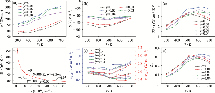
图6
样品(Ag1-yNbyBiSe2)0.75(SnTe)0.25的热电性能
Fig. 6
Thermoelectric properties of (Ag1-yNbyBiS e2)0.75(SnTe)0.25 samples
Temperature dependent (a) electrical conductivity, (b) Seebeck coefficient, (c) power factor, (e) total and lattice thermal conductivity, and (f) ZT; (d) Absolute value of the Seebeck coefficient as a function of Hall carrier concentration at ambient conditions
表1 (Ag1-yNbyBiSe2)0.75(SnTe)0.25样品的载流子浓度n和迁移率μ
Table 1
| Sample | n/cm-3 | μ/(cm2·V-1·s-1) |
|---|---|---|
| y=0 | 1.12×10²⁰ | 2.98 |
| y=0.01 | 1.33×10²⁰ | 2.99 |
| y=0.02 | 3.36×10²⁰ | 2.65 |
| y=0.03 | 5.92×10²⁰ | 1.38 |
| y=0.04 | 2.14×10²⁰ | 2.93 |
3 结论
本研究采用真空熔融结合放电等离子体烧结技术分别制备了(AgBiSe2)1-x(SnTe)x(x=0.10~0.30)和(Ag1-yNbyBiSe2)0.75(SnTe)0.25(y=0.01~0.04)材料, 系统研究了SnTe与AgBiSe2进行合金化对其物相结构和热电性能的影响, 以及Nb掺杂对立方相结构(AgBiSe2)0.75(SnTe)0.25化合物热电性能的影响。研究结果表明, SnTe与AgBiSe2进行合金化不仅可以降低立方相相变温度还可以有效抑制可逆相变, 当SnTe含量为0.25时, AgBiSe2在300~700 K的温度范围内可以维持稳定的立方相结构, 并且室温晶格热导率从0.76 W·m-1·K-1降低到0.51 W·m-1·K-1。同时, Ag位掺杂Nb元素, 在提高载流子浓度的基础上, 引入了点缺陷, 不仅进一步优化材料的电学性能, 还使得高温范围内的晶格热导率显著降低。700 K条件下, 从0.56 W·m-1·K-1(未掺杂)降低至0.43 W·m-1·K-1(Nb掺杂量为0.04)。最终获得了立方相结构稳定的(Ag0.98Nb0.02BiSe2)0.75(SnTe)0.25材料, 其在650 K时ZT达到0.32。上述研究结果为解决高性能热电材料的相变问题进行了有益的探索, 有助于进一步推动其应用进程。
参考文献
Seebeck-driven transverse thermoelectric generation
Efficiency in thermoelectric generators based on Peltier cells
Preparation and characterization of Ag2Se-based ink used for inkjet printing

Preparation of silver selenide (Ag2Se) based thin films is significant to the micro devices. However, most of reported methods for preparing Ag2Se films have not achieved the accuracy control and flexible pattern design of films. Inkjet printing technology is believed to provide a valid approach to solve this problem by which combination Ag2Se and inkjet printing technology shows high value and importance. In this work, Ag2Se nanoparticles were synthesized by solvothermal method and then dispensed into different solvents to obtain the ink with high stability. Jetting parameters were further developed to achieve the jetting of Ag2Se ink and optimize the morphology of droplets. Ag2Se thin films were prepared on polyimide substrates via inkjet printing with different printing layers. As-printed films were finally annealed to increase the crystalline and density. The phase and surface morphology of Ag2Se films were characterized and the electrical conductivity of the films was measured by using four-probe measurement. Ag2Se films can achieve higher density and crystallinity with ink concentration and printing layers increasing, which leads to higher electrical conductivity. Improvement of structure and performance of Ag2Se films result from the increasing deposition and stacking density of Ag2Se nanoparticles. The electrical conductivity of inkjet-printed Ag2Se film can reach as high as 399 S·cm-1 at the ink concentration of 5 mg·mL-1 and the number of printing layers of 40, which provides a new orientation to prepare Ag2Se based films and devices.
Research progress on crystal growth and the thermoelectric properties of Zintl phase Mg3X2(X= Sb, Bi) based materials
Realization of high thermoelectric performance in n-type partially filled skutterudites
An instant change of elastic lattice strain during Cu2Se phase transition: origin of abnormal thermoelectric properties
Thermoelectric materials: energy conversion between heat and electricity
Atomic and electronic structures of I-V-VI2 ternary chalcogenides
The impact of lone-pair electrons on the lattice thermal conductivity of the thermoelectric compound CuSbS2
Synthesis and transport property of AgSbTe2 as a promising thermoelectric compound
Polycrystalline AgSbTe2 ternary compound materials with high phase purity were fabricated using a combined process of mechanical alloying and spark plasma sintering. It was found that stoichiometric AgSbTe2 is a promising composition for low-and-mediate temperature applications, whose ZT reaches 1.59 at 673K, benefiting from its extremely low thermal conductivity (0.30W∕mK) in addition to its low electrical resistivity (<1.1×10⁻⁴Ωm) and large positive Seebeck coefficient (260μV∕K). On the other hand, deviating from this formula would lead to unstable phase structures and higher thermal conductivity, which make the samples less attractive as thermoelectric materials or components of thermoelectric systems.
Enhanced atomic ordering leads to high thermoelectric performance in AgSbTe2
Enhanced thermoelectric performance in p-type AgSbSe2 by Cd-doping
Enhancement of thermoelectric properties by Na doping in Te-free p-type AgSbSe2
Vacancy and anti-site disorder scattering in AgBiSe2 thermoelectrics
In-situ growth of carbon nanotubes on ZnO to enhance thermoelectric and mechanical properties
As a high-temperature thermoelectric (TE) material, ZnO offers advantages of non-toxicity, chemical stability, and oxidation resistance, and shows considerable promise as a true ready-to-use module under air conditions. However, poor electrical conductivity and high thermal conductivity severely hinder its application. Carbon nanotubes (CNTs) are often used as a reinforcing phase in composites, but it is difficult to achieve uniform dispersion of CNTs due to van der Waals forces. Herein, we developed an effective in-situ growth strategy of homogeneous CNTs on ZnO nanoparticles by exploiting the chemical vapor deposition (CVD) technology, in order to improve their electrical conductivity and mechanical properties, as well as reducing the thermal conductivity. Meanwhile, magnetic nickel (Ni) nanoparticles are introduced as catalysts for promoting the formation of CNTs, which can also enhance the electrical and thermal transportation of ZnO matrices. Notably, the electrical conductivity of ZnO is significantly boosted from 26 to 79 S·cm−1 due to the formation of dense and uniform conductive CNT networks. The lattice thermal conductivity (κL) is obviously declined by the intensification of phonon scattering, resulting from the abundant grain boundaries and interfaces in ZnO-CNT composites. Importantly, the maximum dimensionless figure of merit (zT) of 0.04 at 800 K is obtained in 2.0% Ni-CNTs/ZnO, which is three times larger than that of CNTs/ZnO prepared by traditional ultrasonic method. In addition, the mechanical properties of composites including Vickers hardness (HV) and fracture toughness (KIC) are also reinforced. This work provides a valuable reference for dispersing nano-phases in TE materials to enhance both TE and mechanical properties.
Mg3(Bi,Sb)2-based thermoelectric modules for efficient and reliable waste-heat utilization up to 750 K
High thermoelectric properties of n-type AgBiSe2
We report on the thermoelectric (TE) performance of intrinsic n-type AgBiSe2, a Pb-free material with more earth-abundant and cheaper elements than intrinsic p-type homologous AgSbTe2. Pb doping changes n-type AgBiSe2 to p-type but leads to poor electrical transport properties. Nb doping enhances the TE properties of n-type AgBiSe2 by increasing the carrier concentration. As a result of the intrinsically low thermal conductivity (0.7 W m(-1) K(-1)), low electrical resistivity (5.2 mΩ cm), and high absolute Seebeck coefficient (-218 μV/K), the TE figure of merit (ZT) at 773 K is significantly increased from 0.5 for solid-state-synthesized pristine AgBiSe2 to 1 for Ag0.96Nb0.04BiSe2, which makes it a promising n-type candidate for medium-temperature TE applications.
Enhanced thermoelectric performance of n-type transformable AgBiSe2 polymorphs by indium doping
We demonstrate the improved thermoelectric properties of n-type lead-free transformable AgBiSe2 polymorphs by indium doping on silver sites. X-ray diffraction analysis suggests that complete solid solutions are well formed up to [In] = 0.02. Electrical conductivity and Seebeck coefficient behave in a routinely opposite manner due to the dominant role of the carrier concentration adjusted by the localized indium impurity levels, as also suggested by our density functional theory (DFT) calculations. As indium concentration increases, we observe a drastic variation of the thermoelectric transport properties with temperature, in the range of 450 to 580 K. By performing the isothermal electrical measurements, we attribute this interesting behavior to the ongoing α to β phase transformation process. The In 5s lone pair electrons, as indicated from our DFT calculations, increase the anharmonicity of the chemical bonds and enhance the phonon-phonon scattering. This, together with the introduced InAg.. point defects, further brings down the lattice thermal conductivity. The maximum thermoelectric figure of merit ZT is achieved at 773 K and increases from 0.3 for pristine AgBiSe2 to 0.7 for an optimal [In] = 0.015 doping, a more than two times enhancement.
Ultralow thermal conductivity in n-type Ge-doped AgBiSe2 thermoelectric materials
Promising thermoelectric performance in n-type AgBiSe2: effect of aliovalent anion doping
High thermoelectric performance of tellurium-free n-type AgBi1-xSb Se2 with stable cubic structure enabled by entropy engineering
Structural phase transition and related thermoelectric properties in Sn doped AgBiSe2
AgBiSe2, which exhibits complex structural phase transition behavior, has recently been considered as a potential thermoelectric material due to its intrinsically low thermal conductivity. In this work, we investigate the crystal structure of Sn-doped AgBiSe2 through powder X-ray diffraction and differential scanning calorimetry measurements. A stable cubic Ag1−x/2Bi1−x/2SnxSe2 phase can be obtained at room temperature when the value of x is larger than 0.2. In addition, the thermoelectric properties of Ag1−x/2Bi1−x/2SnxSe2 (x = 0.2, 0.25, 0.3, 0.35) are investigated, revealing that Ag1−x/2Bi1−x/2SnxSe2 compounds are intrinsic semiconductors with a low lattice thermal conductivity. This work provides new insights into the crystal structure adjustment of AgBiSe2 and shows that Ag1−x/2Bi1−x/2SnxSe2 is a potentially lead-free thermoelectric material candidate.
Inhibition of lattice thermal conductivity of ZrNiSn-based half-Heusler thermoelectric materials by entropy adjustment
The thermoelectric properties of ZrNiSn-based half-Heusler materials were hindered due to their high thermal conductivity. In order to reduce the lattice thermal conductivity, the high-entropy alloys ZrNiSn and Zr0.5Hf0.5Ni1-xPtxSn (x=0, 0.1, 0.15, 0.2, 0.25, 0.3) were prepared by levitation melting and spark plasma sintering. Configurational entropy of the alloys was manipulated by Hf substitution for Zr and Pt substitution for Ni. Effects of configuration entropy on the thermoelectric properties were investigated. The reslults showed that the minimum sum of lattice thermal conductivity and bipolar thermal conductivity (κl+κb) at 673 K for Zr0.5Hf0.5Ni0.85Pt0.15Sn was optimized at 2.1 W·m-1·K-1, which was significantly reduced by about 58% when compared with ZrNiSn. This finding provides an effective strategy for reducing lattice thermal conductivity of ZrNiSn-based alloy to offer great potential for further improvement of thermoelectrics.
Entropy engineered cubic n-type AgBiSe2 alloy with high thermoelectric performance in fully extended operating temperature range
Revised effective ionic radii and systematic studies of interatomie distances in halides and chaleogenides
Polymorphism in some IV-VI compounds induced by high pressure and thin-film epitaxial growth
The NaCl structures PbS, PbSe, PbTe and SnTe have been found to transform to a Pnma orthorhombic (distorted NaCl) structure under high pressures. Epitaxial growth on rock salt of thin films of normally orthorhombic (Pnma) SnS, SnSe and PbSnS2 induces NaCl structures. There exists a close correlation between the lattice constants of the corresponding NaCl and the orthorhombic polymorphic structures of the Pb and Sn compounds.
Effects of AgBiSe2 on thermoelectric properties of SnTe
Effect of Te and In co-doping on thermoelectric properties of Cu2SnSe3 compounds
Chemical composition engineering leading to the significant improvement in the thermoelectric performance of AgBiSe2-based n-type solid solutions
Stabilized cubic phase BiAgSe2-xSx with excellent thermoelectric properties via phase boundary engineering
Strong lattice anharmonicity securing intrinsically low lattice thermal conductivity and high performance thermoelectric SnSb2Te4 via Se alloying
