

为了实现神经形态计算的人工突触和神经元, 研究人员做了大量的前期研究[5⇓⇓⇓⇓⇓⇓⇓-13]。两端结构的忆阻器[9-10,12-13]和多端口结构的神经形态晶体管[6,11]均已被用来模拟生物突触计算功能。由金属/绝缘体/金属结构组成的忆阻器具有良好的可扩展性、大连接性、低能耗以及与互补金属氧化物半导体(CMOS)工艺的良好兼容性等特性[14]。但是两端结构的忆阻器, 信号写入和读取不能同时进行。相比之下, 多端口结构的神经形态晶体管能同步实现信号传输以及权重更新和学习。另外, 有研究报道表明, 基于晶体管结构的突触器件在实现线性可塑性方面比忆阻器更具前途[15-16]。需要注意的一点是, 目前大部分研究都是基于刚性衬底制备的神经形态器件[5-6,8]。传统的刚性神经形态晶体管很难密切贴合柔软、弯曲的人体, 通常会在超低应变(约1%)下断裂[7], 这会严重限制其在某些实际领域的应用, 比如人体皮肤和植入治疗等[17-18]。而具有良好弯曲特性的柔性神经形态晶体管不仅可以同时实现信号传输和训练学习, 对多路信号进行非线性时空整合与协同调控, 而且能够密切贴合柔软的人体皮肤, 承受器官和组织的高生理应变。更重要的是, 柔性神经形态晶体管设计灵活,具有优异的生物兼容性, 在检测生物环境中生理相关时间尺度的低幅信号方面具备独特的优势和应用潜力。近年来, 伴随半导体材料与器件技术的高速发展, 晶体管的性能已大幅提升, 与柔性衬底相匹配的制备工艺逐步成熟, 在柔性衬底上构建高密度高性能阵列也成为可能。在神经信号监测方面, 柔性神经形态晶体管更体现出天然优势, 有望突破当前刚性电极和刚性晶体管的结构限制, 为深入探索大脑奥秘做出贡献。到目前为止, 已经有大量的综述文献聚焦于柔性神经形态器件, 但基本都是基于柔性神经形态器件的类型(忆阻器、浮栅晶体管、铁电晶体管等)或者功能(仿生感知、神经形态计算等)进行分类叙述。而制备柔性神经形态晶体管的第一步就是柔性衬底的选择, 本文主要综述近年来基于不同柔性衬底的神经形态晶体管研究进展, 然后介绍目前研究使用的各种柔性衬底, 及其研制的柔性神经形态晶体管的特性和应用。最后, 展望了柔性神经形态晶体管的未来发展。
1 突触晶体管
2009年, Wan等[19]采用低温等离子体增强化学气相沉积制备了SiO2纳米颗粒膜, 该薄膜是一种质子导电的固态电解质薄膜并具有非常大的单位面积双电层电容。在后续研究中, Wan等研制了一系列新结构的氧化物双电层晶体管, 并探索了该类新概念器件在仿生传感器与神经形态器件领域的应用。氧化物双电层晶体管就是一类利用电解质作为栅介质、氧化物半导体作为沟道的薄膜晶体管。在外电场作用下, 电解质中的离子发生迁移, 在电解质与半导体界面处聚集, 诱导半导体中产生载流子, 形成巨大的双电层电容, 从而有效地降低晶体管的工作电压。这种离子/电子耦合的器件的工作原理与信息在突触结构中传递的过程类似, 因此在模拟突触功能方面具有较大的优势。2010年, Chen等[20]通过集成离子/电子混合材料制备了多端口神经形态晶体管, 成功模拟了具有尖峰信号处理、学习和记忆功能的生物突触性能。自此, 突触晶体管的研究越来越多。图1展示了双电层突触晶体管的示意图以及对应的生物突触示意图。具有源极漏极的活性层被认为是突触后端, 它受突触晶体管栅电极突触前端的调节。同时, 突触后端的变化被认为是突触的权重变化, 与突触晶体管的电荷存储能力有关[21]。
图1
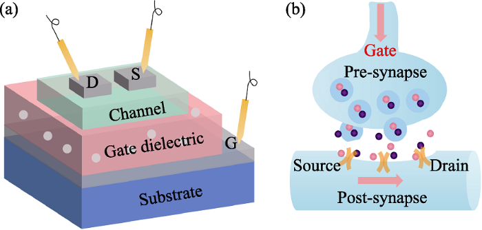
图1
双电层突触晶体管(a)和生物突触(b)的示意图
Fig. 1
Schematic diagrams of electric-double-layer synaptic transistor (a) and biological synapse (b)
在神经网络中, 突触前神经元和突触后神经元之间的连接强度被定义为突触权重, 突触权重可以通过动作电位来调节(即突触可塑性)[21]。一般来说,突触可塑性可分为短程可塑性(STP)和长程可塑性(LTP)[22⇓⇓⇓-26]。STP是突触连接的一种暂时性变化, 去除外部钉刺后会迅速衰减到原始状态, 这是信息处理不可或缺的。当电位脉冲作用于突触前膜时, 神经递质被释放, 导致突触后的电流变化。兴奋性突触后电流(EPSC)在兴奋性神经递质释放时产生, 增强突触权重。而抑制性突触后电流(IPSC)在抑制神经递质释放时产生, 减弱突触权重。双脉冲易化(PPF)是典型的STP行为之一, 它描述的是连续施加一对突触前脉冲获得增强的突触后反应[27]。相比之下, LTP是突触连接的长期转化, 对记忆和学习至关重要。除了对突触可塑性进行分类外, 影响突触可塑性的因素也值得研究。时间尖峰依赖的可塑性(STDP)和频率依赖的可塑性(SRDP)是改变突触权重的两个主要因素, 它们都是神经网络的基本学习规则[28]。
2 基于不同柔性衬底的突触晶体管
选择柔性衬底对突触晶体管的机械应变和突触性能有重要影响。 常见的柔性高分子材料衬底包括聚酰亚胺(PI)[29⇓⇓-32]、 聚萘二甲酸乙二醇酯(PEN)[33⇓⇓⇓-37]、 聚对苯二甲酸乙二醇酯(PET)[38⇓⇓-41]和聚二甲基硅氧烷(PDMS)。除此之外, 还有一些常用的柔性衬底, 比如云母、壳聚糖等。这些衬底材料各自有其优缺点。而在构建柔性突触晶体管时, 可以根据以下几点选择合适的衬底: a)器件的制备工艺, 比如在制备过程中, 需要经过高温, 那么需要选择耐高温的柔性衬底(如云母); b)器件的应用方面, 比如器件需要透光性测试, 那么需要选择柔性透明的衬底(如PEN); c)生物可降解, 如果需要考虑环境污染, 那么柔性的纸基衬底是一个不错的选择。总的来说, 在构建柔性突触晶体管时,需要从器件的制备、测试和应用等方面考虑选择最合适的柔性衬底。
2.1 基于PI衬底的突触晶体管
PI是指高分子主链上含有亚胺环结构的一类有机高分子聚合物, 有很多种类。PI分子中的芳杂环结构十分稳定, PI薄膜在300 ℃的高温下也表现出很高的稳定性。因此, 用PI作为柔性突触晶体管的衬底有利于提高突触晶体管器件在高温环境下的热稳定性。然而PI呈橙色, 透明度相对较差, 图2(a)为基于PI衬底制备的人造突触晶体管的实物照片[29]。2019年, Zhang等[30]在自制的PI衬底上制备了一种新型柔性双栅突触晶体管。图2(b)展示了该器件在不同光强度脉冲下的EPSC响应, 可以明显看到, 施加光脉冲时EPSC突然增加, 而去除光脉冲后EPSC逐渐衰减到初始状态, 并且最大EPSC可以通过光脉冲的强度来控制。更重要的是, 该器件可以通过光和电的协同调制, 调节人工突触的记忆水平。而用不同的电压调节光输入的记忆保持水平, 与视神经系统的功能类似。也就是说, 该柔性突触晶体管提供了一种模仿视觉记忆的新想法, 为未来的电子眼提供了一种有前途的策略。2020年, Wan等[31]在PI衬底上制备了具有神经形态功能的柔性多栅铟镓锌氧化物(IGZO)薄膜晶体管。如图2(c)所示, 当施加在侧栅上的调制电压从-1.0 V增加到1.0 V时, EPSC振幅从4.2 nA增加到32.0 nA。栅压可以调节EPSC的振幅, 这对于动态突触权重调制来说非常重要, 不仅薄膜突触晶体管表现出优异的生物突触性能, 而且由纳米纤维制备的柔性突触晶体管的性能也不相上下。最近, Shan等[29]在PI衬底上集成了基于In2O3纳米纤维的柔性突触晶体管, 以壳聚糖溶液为栅介质的突触晶体管成功模拟了突触行为, 如短程可塑性和长程可塑性。该柔性突触晶体管表现出良好的生物相容性, 并且通过混合的国家标准和技术研究所(MNIST)数据库对手写数字的模拟器件阵列的模式识别率高达92%, 如图2(d)所示。这表明柔性突触晶体管具有良好的模式识别性能。2021年, Park等[32]在PI衬底上成功制备了基于硅铟锌氧化物的柔性人工突触, 该柔性突触器件在高机械(弯曲1500次, 半径5 mm)和电应力(电压脉冲104次)下表现出极其稳定的突触性能。他们还提出了一种由可拉伸电阻传感器和灵活的人工突触组成的手语翻译感觉神经形态系统的新概念, 该系统可以为聋人提供直接和实时的手语翻译。利用可拉伸传感器获得的手势模式进行训练和识别仿真, 验证了该系统的可行性, 优化后的特征识别率最高可达99.4%。更重要的是,即使在物理弯曲条件下,识别率也超过90%。这一结果可能为未来建立可穿戴感觉神经形态系统奠定坚实的基础。
图2
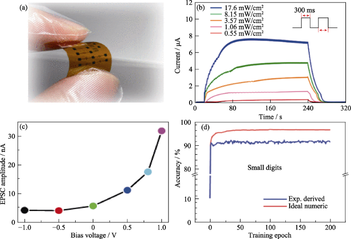
图2
基于PI衬底的突触晶体管的研究工作
Fig. 2
Research on synaptic transistor on PI substrate
(a) Image of In2O3 nanofiber synaptic transistor on PI substrate[29]; (b) Optical response of EPSC triggered by different light intensities[30]; (c) Relationship between amplitude of EPSC response to presynaptic peak (2.0 V, 25 ms) and gate pressure[31]; (d) Accuracy of simulated neural network for pattern recognition of MNIST small digit (8×8 pixels) database[29]; Colorful figures are available on website
2.2 基于PEN衬底的突触晶体管
PEN是一种新型的高性能聚酯材料,熔点在260~270 ℃, 能在100 ℃环境中长期使用[33]。不仅如此, PEN还具有优异的机械柔韧性、耐腐蚀性、化学稳定性、绝缘性、透明性和耐水解性[34]。PEN不仅作为音膜材料应用于耳机膜和音响振膜等领域, 而且在5G产业也有广泛的应用, 是制作柔性线路板(FPC)的良好材料之一[35]。最近, Xu等[36]基于PEN衬底制备了一种电光调制的突触器件, 图3(a)展示了该突触晶体管示意图。这也是首次使用了一种特殊的纳米粒子导电通道, 用于模拟类似大脑的处理过程和神经感知功能。从图3(b)可以明显看出, 其电信号突触(EPS)阵列在机械上也具有良好的灵活性, 经过10000次弯曲后, 突触后电流保持了初始值的41.8%, 这也是迄今为止柔性突触晶体管的最大弯曲循环数。更重要的是, 作为一种神经光学传感突触晶体管, 它能在毫伏读取电压下对不同强度和持续时间的紫外光产生反应, 并作为痛觉感受器实现疼痛感知。图3(c)是提出的紫外线刺激引起的疼痛感知模型示意图。从图3(d)可以看出, 随着紫外光增强, 疼痛指数也在增加。但随着连续紫外线照射间隔时间延长, 这种促进作用减弱, 但疼痛反应仍然存在(图3(e))。这种纳米粒子突触晶体管作为痛觉感受器的尝试可能在新的人工感觉系统中有潜在的应用价值。2022年, Zhang等[37]也使用PEN衬底构建了光突触晶体管, 该突触晶体管不仅具有极低的工作电压和电流, 还具有非凡的神经形态光感知能力。因此, 该器件成功地模拟了视觉神经对外部光刺激的反应, 短程可塑性中的超低能耗为0.07~34 fJ/spike, 长程可塑性中的超低能耗为0.41~19.87 fJ/spike, 两者都接近生物突触的能效(1~100 fJ)。此外, 在柔性衬底上的8×8突触晶体管阵列构成的人工光学-神经网络以较低的能量消耗显示出优异的图像识别和增强能力。也就是说, 该突触晶体管提供了一个以极低的能量消耗实现光子神经形态功能的方法。
图3
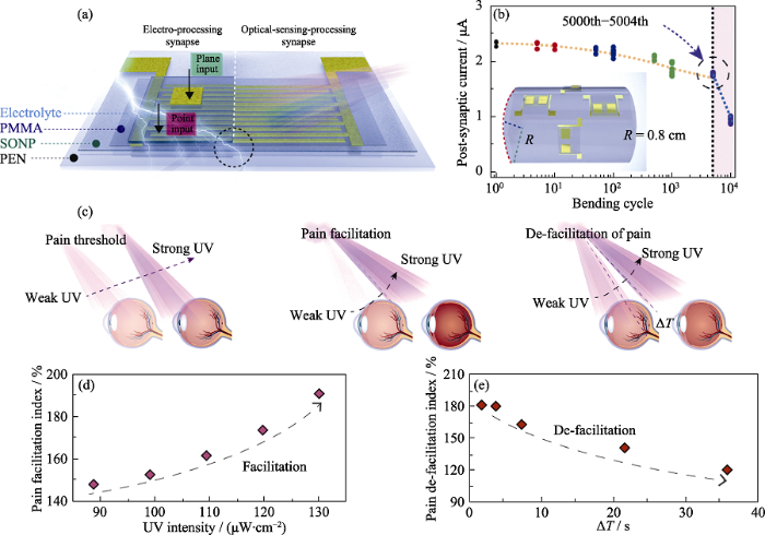
图3
基于PEN衬底的突触晶体管的研究工作[36]
Fig. 3
Research on synaptic transistor on PEN substrate[36]
(a) Schematic diagram of a synaptic transistor constructed on a PEN substrate; (b) Variation trend of the postsynaptic current with the number of bending, and curvature radius at 0.8 cm during the test; (c) Schematic diagram of a pain perception model caused by UV stimulation; (d) Pain facilitation index increased with the increase of UV intensity; (e) Change of pain de-facilitation index with ΔT
2.3 基于PET衬底的突触晶体管
PET具有极高的透明度, 其长期使用温度在80 ℃左右[38]。图4(a)展示了基于PET衬底构建的突触晶体管的实物照片[39]。2013年, Wan等[40]通过简单的自组装方法在PET衬底上构建了基于铟锌氧(IZO)的柔性突触晶体管。研究发现, 当高栅脉冲(4.0 V, 20 ms)应用于ITO栅电极时, 该突触晶体管可以实现非易失性记忆和长程可塑性。图4(b)显示了20个栅压(4.0 V, 20 ms)脉冲刺激的EPSC随时间的变化。初始突触电流约为8.0 nA, 可逐渐增大至最大11.9 μA。去除脉冲后可测到较高的突触后电流 (>5.0 μA)。除此以外, 该柔性人工突触晶体管的PPF和长程记忆也受到了关注。这种基于IZO的柔性电子突触有望用于构建神经形态系统。2014年, Wan等[40]又在PET衬底上制备了柔性铟镓锌氧(IGZO)双电层晶体管。该类IGZO柔性突触晶体管在高能效的神经形态系统和脑机接口应用中具有广阔的前景。不仅如此, Li等[41]更是基于PET衬底制备了一种双栅电解质的人工异质结突触晶体管, 它可以实现实时时空信息的集成和存储。图4(c)展示了执行时空信号整合和记忆的异质突触示意图。从图4(d)可以明显看出, 与单栅突触晶体管相比, 采用异质结突触晶体管的MNIST手写数字分类精度由89.3%提高到99.0%。该研究结果表明, 多栅异质结突触晶体管在模拟复杂时空信息处理功能方面具有巨大的潜力, 并能为先进神经形态计算系统设计提供新的平台。更重要的是, 这些结果为在物理器件中高效地实现复杂生物异质突触功能开辟了新的途径, 并有可能用于柔性智能可穿戴系统。不过使用这些概念验证设备还需要实现设备最小化和高密度集成。
图4
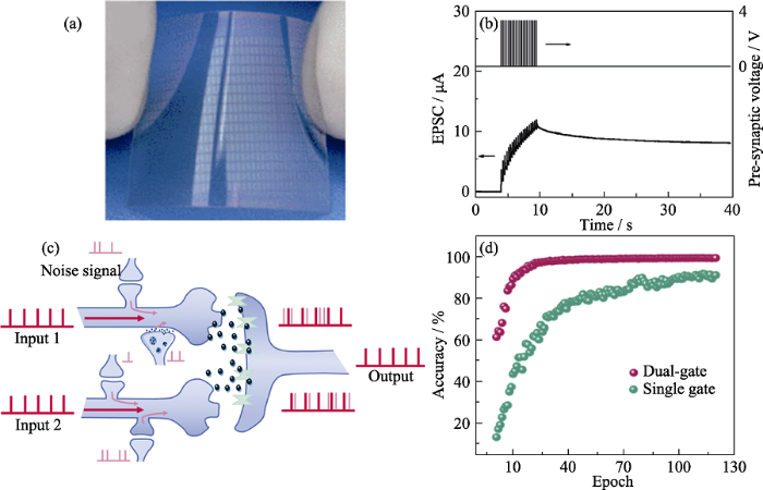
图4
基于PET衬底的突触晶体管的研究工作
Fig. 4
Research on synaptic transistor on PET substrate
(a) Physical photograph of the construction of synaptic transistors on a PET substrate; (b) Change of current with time after 20 (4.0 V, 20 ms) pulses being applied to the gate of the synaptic transistor when VDS at 0.5 V [39]; (c) Schematic diagram of spatio-temporal signal integration and memory performed by heterogeneous synapses (with the introduction of noise signals during the transmission of the original signal); (d) Comparison of classification accuracy of two-gate heterogeneous synaptic transistor and single-gate homogeneous synaptic transistor networks[41]
2.4 基于云母衬底的突触晶体管
云母是一种众所周知的天然无机晶体, 具有成本低、柔韧性好、透光性高、介电强度高、热稳定性好等优点[42-43], 已被广泛应用于电子工业领域,例如, 射频设备的电容器、高压电气设备的绝缘体以及薄层低热阻绝缘体[44]。有趣的是, 云母在原子水平上是平的, 可作为原子力显微镜(AFM)校准的标准样品[43]。更重要的是, 云母耐高温((600±20) ℃), 很多铁电薄膜需要经过高温退火(>400 ℃), 才能结晶成铁电相, 所以云母作为铁电晶体管器件的理想衬底, 引起了广泛关注[45⇓⇓-48]。2020年, Li等[45]基于云母衬底制备了一个全无机柔性人工突触晶体管(云母/SRO/PZT/IGZO异质结构)。从图5(a)可以发现, 该器件具有出色的突触特性。不仅如此, 该器件还具有显著的机械灵活性和高温可靠性。当弯曲半径减小到4.0 mm时, 循环测试达到400次; 当测试温度达到100 ℃时, 器件的突触行为几乎没有变化。此外, 该器件的MNIST手写数字识别精度可达94.4%。这项工作为实现灵活、低功耗、高效的模拟大脑的神经形态计算提供了一种很有前途的方法。2021年, Duan等[49]在云母衬底上构建了一个柔性透明的VO2 Mott晶体管, 用于模拟生物突触的功能。图5(b)展示了该突触晶体管的光学照片。随着多种基本突触功能的实现, 该突触晶体管成功模拟了一种重要的感觉神经元。图5(c)为EPSC计数图, 用于评估疼痛强度。更重要的是, 该突触晶体管对弯曲变形具有较高的耐受性, 多导态在增强和下降特性上的周期变化保持在4.0%以内。而且图5(d)的仿真结果显示, 由该突触晶体管构建的卷积神经网络可以达到较高的手写数字识别精度(>95%), 进一步表明该柔性装置适用于神经形态计算。最近, Jeon等[50]基于云母衬底沉积的Hf0.5Zr0.5O薄膜成功制备了柔性铁电突触晶体管。该晶体管经过10000次弯曲循环后, 电学性能的变化可以忽略不计, 具有优异的机械灵活性。而且, 该柔性突触具有线性和对称的增强和抑制特性, 模式识别准确率高达91.44%。
图5
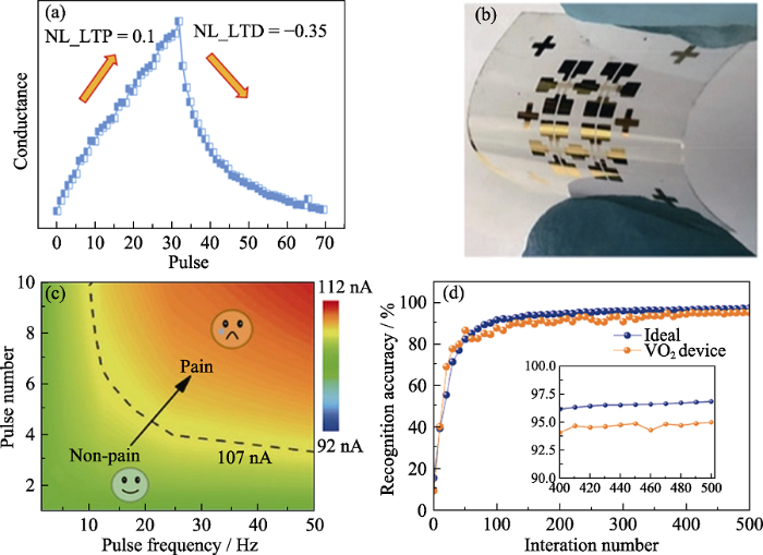
图5
基于云母衬底的突触晶体管的研究工作
Fig. 5
Research on synaptic transistor on mica substrate
(a) Synaptic plasticity of synaptic transistors constructed on mica substrate[45]; (b) Optical photographs of flexible VO2 transistors constructed on mica substrate; (c) EPSC count chart to assess pain intensity; (d) Simulation identification accuracy of ideal devices and VO2 transistor devices[49]; EPSC: Excitatory post-synaptic current
2.5 基于纸基衬底的突触晶体管
纸作为人类历史上最伟大的发明之一, 一直在人类历史中发挥着重要的作用。随着科技进步, 纸又被开发出了新的功能, 比如作为柔性光电器件的衬底[51-52]。纸衬底具有柔软可弯曲、可循环利用、价格低廉和可生物降解等优异特性。但也有一个致命的缺陷——不耐高温, 所以使用其制备突触晶体管时, 不仅在制备器件过程中, 而且在测试使用过程中, 均以室温下为宜。早在2014年, 就有研究者在纸衬底上构建了突触晶体管[52]。Jiang等[52]以纸为衬底, 制备了以质子酸掺杂的壳聚糖为栅介质, 氧化铟锌(IZO)为沟道材料的突触晶体管。图6(a)展示了该突触晶体管的原理示意图, 图6(b)为纸衬底上弯曲突触晶体管的光学照片。由于具有脉冲电压响应的质子在壳聚糖电介质中的运动, 纸突触晶体管成功模拟了生物突触功能, 包括兴奋性突触后电流、双脉冲易化、动态滤波和时空相关信号处理 (图6(c, d))。他们的研究结果有力地证明了这种纸基突触晶体管不仅对构建廉价和生物友好的人工神经元网络很重要, 而且对实现智能生物材料也很有意义。另外, Wan等[53]也基于纸衬底制备了以SiO2纳米颗粒薄膜为栅介质, IZO为沟道材料的双电层薄膜晶体管, 研究结果表明, 这种柔性IZO晶体管可作为人工突触装置, 并证明了突触的刺激响应和短程突触可塑性功能。这种基于IZO的纸基双电层薄膜晶体管可能在低功率纸电子、柔性人工突触和神经形态系统中有潜在的应用。
图6

图6
基于纸衬底的突触晶体管的研究工作[52]
Fig. 6
Research on synaptic transistor on paper substrate[52]
(a) Schematic diagram of the chitosan /IZO synaptic transistor constructed on paper substrate; (b) Optical photographs of bent synaptic transistors on a paper substrate; (c, d) Simulated biological synaptic function on paper synaptic transistors
2.6 基于其他自支撑柔性衬底的突触晶体管
除了上述提到的柔性衬底外, 还有一些自支撑的柔性衬底, 比如PDMS[54]、海藻酸钠膜[55]、壳聚糖[56-57]等。Guo等[54]使用PDMS为衬底, 以P3HT-NF作为半导体演示了可拉伸的有机突触晶体管, 首次研究了在不同变形状态下机械变形对其突触行为的影响。从图7(a)可以明显看出, 可拉伸突触晶体管表现出优异的机械稳定性。他们的研究结果表明, 生物感觉神经元最重要的参数: 突触晶体管的学习、记忆行为和衰减常数, 可以通过机械形变调节, 这与离子凝胶中依赖机械变形的离子传输有关。 这些结果为利用机械变形开发不同功能器件提供了一个很有前途的方向。另外, Wan等[56]在壳聚糖膜上制备了具有双栅结构的IZO神经形态晶体管, 并用于柔性人工痛觉感受器模拟。图7(b)显示了独立人工痛觉感受器在不同调制电压下的疼痛阈值。疼痛阈值可调的人工伤害感受器可以提高周围复杂环境中的检测效率。图7(c)显示了调制电压依赖性疼痛反应。这种疼痛反应可调的人工痛觉感受器可以帮助失去知觉的患者感受疼痛, 也可以帮助对疼痛敏感的人减轻疼痛感。这种独立的仿生装置不仅能将疼痛感知功能捕捉到外周输入, 还可以通过施加在第二栅极上的电压来模拟疼痛敏感性的调制。2021年, Wan等[57]又基于壳聚糖衬底构建了双栅MoS2神经形态晶体管。壳聚糖膜同时用作电介质和基底。该双栅晶体管在柔性壳聚糖膜上不仅表现出较高的机械稳定性和电学性能, 还成功仿真了一些重要的突触功能, 如成对脉冲易化和可调高通滤波器。该结果极大地丰富了二维柔性电子学和神经形态感知系统的研究。最近, Chen等[58]基于PEF(生物基材料)衬底, 制备了一个突触晶体管, 它将光响应从可见光扩展到紫外到近红外光, 并模拟了人类在宽多波长光刺激下的视觉感知、记忆和光学数据处理。该研究不仅展示了生物复合材料在人工突触中的应用潜力, 还可为设计高性能的人工突触光电晶体管提供有效的指导。
图7
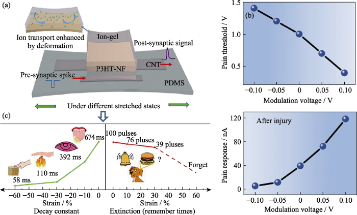
图7
基于其他自支撑柔性衬底的突触晶体管的研究工作
Fig. 7
Research on synaptic transistor on other self-support substrate
(a) Organic synaptic transistor based on PDMS substrate and its excellent mechanical stability[54]; (b) Pain thresholds of independent artificial nociceptors at different modulation voltages; (c) Pain response currents of independent artificial nociceptors at different modulation voltages[56]
3 柔性神经元晶体管
神经元与神经元之间通过突触连接。突触后神经元通过整合来自其它神经元的信号, 然后产生简单的输出形式: 动作电位[59], 从而完成神经元计算功能。早在1992年, Shibata等[60]就提出了具有多个栅极的硅基神经元晶体管。神经元晶体管的“开”或“关”状态取决于多个输入信号的综合效应。值得注意的是, 神经元晶体管是利用电容耦合效应进行操作, 故功耗极低。从那时起, 神经元晶体管就因其阈值电压易于调节而在化学和生物检测中备受关注[61-62]。2013年, Wan等[61]受生物神经元的树突整合和尖峰操作的启发, 在柔性PET衬底上制造了具有多个输入门的柔性氧化物基神经形态晶体管, 并将其应用于pH传感器。图8(a)展示了在双栅协同调制模式下测量该器件pH灵敏度的测量示意图。从图8(b)可以明显发现, 当VG1由正值变为负值时, pH敏感性提高。当VG1=−0.6 V时, 得到的最大pH灵敏度为105 mV/pH。他们的研究结果还表明, 单脉冲动态模式可以显著提高pH灵敏度, 并减少响应/恢复时间和功耗。该柔性神经形态晶体管为生物化学检测提供了一个高灵敏度、快速响应和超低功耗的新概念传感平台。2022年, Xu等[62]制作了一个可拉伸神经形态晶体管, 它不仅可以感知触觉和视觉信息, 还能模拟神经形态处理能力。他们研究发现, 经过500次训练, 利用40 s曝光的实验增强-抑制结果, 识别准确率可达96.3%, 收敛性较好(图8(c))。而且, 该神经网络在经过足够的训练后可以捕获手势的特征并实现高精度的模式识别 (图8(d))。这项工作提供了一种集成触觉感知、光感知和突触信息处理的人工传入神经的方法, 成为迈向与人体兼容的柔性和神经形态电子器件的重要一步。
图8
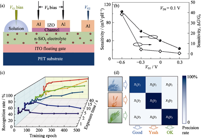
图8
柔性神经元晶体管相关工作
Fig. 8
Research on flexible neuron transistor
(a) Schematic diagram of IZO-based neuron transistor measurement; (b) pH sensitivity of the device with different VG1[61]; (c) Change of the estimated recognition rate of pattern recognition with the number of training under three conditions according to different exposure time; (d) Classification test confusion matrix under three different conditions ("Good", "Yeah" and "OK") after different exposure time and number of iterations[62]
4 结论与展望
在神经形态电子学的发展过程中, 研究人员在设计与制造模拟生物突触的电子器件方面付出了巨大努力。柔性神经形态晶体管因其功耗低、与生物兼容、机械灵活性强等优点,是最适合模拟生物感知突触与神经元的器件。本文综述了近几年基于不同柔性衬底构建的神经形态晶体管的研究进展,从不同的柔性衬底出发, 详细介绍了各种柔性神经形态晶体管的器件结构、能耗、保持力和耐久性等性能参数。除了展示柔性神经形态晶体管的基本突触可塑性外, 还展示了其在神经形态感知与计算领域的应用, 例如神经元树突整合、视觉处理、图像记忆和触觉神经等。从大量文献报道来看, 柔性神经形态晶体管极有可能应用于下一代可穿戴电子设备领域。而且, 随着神经形态晶体管不断进步, 其应用领域也会越来越广泛。在智能感知应用领域, 柔性神经形态晶体管可应用于生物机器人。而在人工神经形态系统的创建方面, 基于柔性神经形态晶体管的人工感觉系统比传统传感器可以更有效地将外部信息传递到大脑。柔性神经形态晶体管还将影响仿生假肢的未来, 可以更好地促进人机融合。柔性神经形态晶体管在生物电子学和神经形态应用方面会继续吸引更多关注。
但遗憾的是, 目前对于柔性神经形态晶体管的研究仍然面临着很多局限性和挑战。1) 目前制备的柔性神经形态晶体管都是单个器件或者小规模阵列, 开发大规模集成的柔性阵列或者芯片仍面临严峻的挑战。2) 利用柔性神经形态晶体管模拟完整的突触功能。到目前为止, 研究人员制备的柔性神经形态晶体管只能模仿生物突触的基本功能。从系统层面来说,人工神经形态器件构建的系统已经实现触觉、视觉、听觉检测等基本功能, 而在一个系统中同时实现多种感知功能的研究相对较少。因此, 多功能神经形态器件对未来低功耗仿生感知系统的发展具有重要意义。3) 柔性神经形态晶体管之间的互连问题。由于生物神经元排列在3D空间中, 突触连接的数量为≈1015, 所以神经形态器件互连将困难重重。4) 柔性神经形态晶体管的能耗问题。在构建人工感觉系统时, 能量效率是要重点考虑的因素。对柔性神经形态晶体管来说, 在单个生物类似刺激脉冲条件下, 能量消耗必须低至每个突触事件1~100 fJ水平。研究人员未来需要更多关注该问题, 选择合适的材料和结构设计或许是降低器件功耗的可行方法。
尽管存在上述困难和挑战, 但可以相信经过研究人员的不断努力, 在不久的将来柔性神经形态晶体管一定会成为智能电子系统的核心单元器件。
参考文献
Flexible neuromorphic electronics for computing, soft robotics, and neuroprosthetics
Memory and learning behaviors mimicked in nanogranular SiO2-based proton conductor gated oxide-based synaptic transistors

In neuroscience, signal processing, memory and learning function are established in the brain by modifying ionic fluxes in neurons and synapses. Emulation of memory and learning behaviors of biological systems by nanoscale ionic/electronic devices is highly desirable for building neuromorphic systems or even artificial neural networks. Here, novel artificial synapses based on junctionless oxide-based protonic/electronic hybrid transistors gated by nanogranular phosphorus-doped SiO2-based proton-conducting films are fabricated on glass substrates by a room-temperature process. Short-term memory (STM) and long-term memory (LTM) are mimicked by tuning the pulse gate voltage amplitude. The LTM process in such an artificial synapse is due to the proton-related interfacial electrochemical reaction. Our results are highly desirable for building future neuromorphic systems or even artificial networks via electronic elements.
Artificial synapses with short-and long-term memory for spiking neural networks based on renewable materials
Flexible, conformal organic synaptic transistors on elastomer for biomedical applications
IGZO nanofiber photoelectric neuromorphic transistors with indium ratio tuned synaptic plasticity
Synaptic plasticity divided into long-term and short-term categories is regarded as the origin of memory and learning, which also inspires the construction of neuromorphic systems. However, it is difficult to mimic the two behaviors monolithically, which is due to the lack of time-tailoring approaches for a certain synaptic device. In this Letter, indium-gallium-zinc-oxide (IGZO) nanofiber-based photoelectric transistors are proposed for realizing tunable photoelectric synaptic plasticity by the indium composition ratio. Notably, short-term plasticity to long-term plasticity transition can be realized by increasing the ratio of indium in the IGZO channel layer. The spatiotemporal dynamic logic and low energy consumption (<100 fJ/spike) are obtained in devices with low indium ratio. Moreover, the symmetric spike-timing-dependent plasticity is achieved by exploiting customized light and electric pulse schemes. Photoelectric long-term plasticity, multi-level characteristics, and high recognition accuracy (93.5%) are emulated in devices with high indium ratio. Our results indicate that such a composition ratio modulated method could enrich the applications of IGZO nanofiber neuromorphic transistors toward the photoelectric neuromorphic systems.
BCM Learning rules emulated by a-IGZO-based photoelectronic neuromorphic transistors
Indium-gallium-zinc-oxide based photoelectric neuromorphic transistors for modulable photoexcited corneal nociceptor emulation
Energy-efficient hybrid perovskite memristors and synaptic devices
Fully memristive neural networks for pattern classification with unsupervised learning
Anisotropic black phosphorus synaptic device for neuromorphic applications
Tailoring transient-amorphous states: towards fast and power-efficient phase-change memory and neuromorphic computing
Stochastic phase-change neurons
Artificial neuromorphic systems based on populations of spiking neurons are an indispensable tool in understanding the human brain and in constructing neuromimetic computational systems. To reach areal and power efficiencies comparable to those seen in biological systems, electroionics-based and phase-change-based memristive devices have been explored as nanoscale counterparts of synapses. However, progress on scalable realizations of neurons has so far been limited. Here, we show that chalcogenide-based phase-change materials can be used to create an artificial neuron in which the membrane potential is represented by the phase configuration of the nanoscale phase-change device. By exploiting the physics of reversible amorphous-to-crystal phase transitions, we show that the temporal integration of postsynaptic potentials can be achieved on a nanosecond timescale. Moreover, we show that this is inherently stochastic because of the melt-quench-induced reconfiguration of the atomic structure occurring when the neuron is reset. We demonstrate the use of these phase-change neurons, and their populations, in the detection of temporal correlations in parallel data streams and in sub-Nyquist representation of high-bandwidth signals.
Memristive physically evolving networks enabling the emulation of heterosynaptic plasticity
Freestanding artificial synapses based on laterally proton-coupled transistors on chitosan membranes
From biomaterial-based data storage to bio-inspired artificial synapse
25th anniversary article: the evolution of electronic skin (e-skin): a brief history, design considerations, and recent progress
Pursuing prosthetic electronic skin
Skin plays an important role in mediating our interactions with the world. Recreating the properties of skin using electronic devices could have profound implications for prosthetics and medicine. The pursuit of artificial skin has inspired innovations in materials to imitate skin's unique characteristics, including mechanical durability and stretchability, biodegradability, and the ability to measure a diversity of complex sensations over large areas. New materials and fabrication strategies are being developed to make mechanically compliant and multifunctional skin-like electronics, and improve brain/machine interfaces that enable transmission of the skin's signals into the body. This Review will cover materials and devices designed for mimicking the skin's ability to sense and generate biomimetic signals.
Ultralow-voltage transparent electric-double-layer thin-film transistors processed at room-temperature
Ionic/electronic hybrid materials integrated in a synaptic transistor with signal processing and learning functions
Oxide-based thin film transistors for flexible electronics
Artificial synaptic transistor with solution processed InOx channel and AlOx solid electrolyte gate
Solar-blind SnO2 nanowire photo-synapses for associative learning and coincidence detection
Artificial synapse emulated by charge trapping-based resistive switching device
Short-term plasticity and long-term potentiation in artificial biosynapses with diffusive dynamics
Noble-metal-free memristive devices based on IGZO for neuromorphic applications
Roles for short-term synaptic plasticity in behavior
Short-term synaptic plasticity is phylogenetically widespread in ascending sensory systems of vertebrate brains. Such plasticity is found at all levels of sensory processing, including in sensory cortices. The functional roles of this apparently ubiquitous short-term synaptic plasticity, however, are not well understood. Data obtained in midbrain electrosensory neurons of Eigenmannia suggest that this plasticity has at least two roles in sensory processing; enhancing low-pass temporal filtering and generating phase shifts used in processing moving sensory images. Short-term synaptic plasticity may serve similar roles in other sensory modalities, including vision.
Long-term synaptic plasticity emulated in modified graphene oxide electrolyte gated IZO-based thin-film transistors
Flexible and compatible synaptic transistor based on electrospun In2O3 nanofibers
Bioinspired flexible, dual-modulation synaptic transistors toward artificial visual memory systems
Flexible oxide-based Schottky neuromorphic TFTs with configurable spiking dynamic functions
Flexible artificial Si-In-Zn-O/ion gel synapse and its application to sensory-neuromorphic system for sign language translation
Flexible artificial synapses are fabricated with a SIZO/ion gel hybrid structure forming a polyimide substrate.
国外印刷电子产业发展概述
近年来印刷电子有了快速发展,许多有关印刷电子的科研成果,已从实验室投入了生产,初步形成了印刷电子产业体系。本文介绍了应用于印刷电子的各类有机、无机材料及工艺装备,特别详细列举了各类印刷电子产品及其应用情况,这些印刷电子产品已开始进入人们日常生活的多个方面。虽然印刷电子产业尚处于发展初级阶段,市场不够成熟,但已显示出十分光明的发展前景。文中还指出政府机构的重视和支持是国外印刷电子产业发展的重要因素。
Flexible electro-optical neuromorphic transistors with tunable synaptic plasticity and nociceptive behavior
A fully solution-printed photosynaptic transistor array with ultralow energy consumption for artificial-vision neural networks
Synaptic behaviors mimicked in flexible oxide-based transistors on plastic substrates
Energy-efficient artificial synapses based on flexible IGZO electric-double-layer transistors
A flexible dual-gate hetero-synaptic transistor for spatiotemporal information processing
Magnetic properties of synthetic fluorophlogopite mica crystals
Mica, a potential two-dimensional-crystal gate insulator for organic field-effect transistors
Flexible electronic synapse enabled by ferroelectric field effect transistor for robust neuromorphic computing
Flexible ferroelectric hafnia-based synaptic transistor by focused-microwave annealing
Highly robust flexible ferroelectric field effect transistors operable at high temperature with low-power consumption
Top-gated MoS₂negative-capacitance transistors fabricated by an integral-transfer of pulsed laser deposited HfZrO2 on mica
A flexible mott synaptic transistor for nociceptor simulation and neuromorphic computing
Flexible ferroelectric hafnia-based synaptic transistor by focused-microwave annealing
Cellulose-based flexible organic light-emitting diodes with enhanced stability and external quantum efficiency
Chitosan-based biopolysaccharide proton conductors for synaptic transistors on paper substrates
Low-voltage protonic/electronic hybrid indium zinc oxide synaptic transistors on paper substrates
Stretchable synaptic transistors with tunable synaptic behavior
Flexible vertical photogating transistor network with an ultrashort channel for in-sensor visual nociceptor
Freestanding dual-gate oxide-based neuromorphic transistors for flexible artificial nociceptors
Flexible dual-gate MoS2 neuromorphic transistors on freestanding proton-conducting chitosan membranes
Harnessing biobased materials in photosynaptic transistors with multibit data storage and panchromatic photoresponses extended to near-infrared band
Neuroscience: exploring the brain, enhanced edition: exploring the brain
A functional MOS transistor featuring gate-level weighted sum and threshold operations
Flexible sensory platform based on oxide-based neuromorphic transistors
