


类脑神经形态计算通过电子或光子器件的集成有效模拟人脑结构, 进而实现人脑功能。人脑是一个高度复杂的神经网络, 包含约1011个神经元和1015个突触, 功耗仅20 W左右[1]。每个神经元通过103~104个突触与其他神经元连接。突触是神经元之间的连接, 大约20~40 nm宽, 通过改变其连接强度可以传递神经元产生的电脉冲[2]。突触是人脑中数量最多的基本信息处理单元, 因此人工突触是类脑计算系统的主要部件。可模拟人工突触的技术有CMOS集成电路[3-4]、晶体管[5-6]、忆阻器[7⇓-9]和自旋电子器件[10]等。其中, 忆阻器具有简单两端结构、优异的尺寸缩放性、超低功耗、超快运行速度等优势, 逐渐成为人工突触的研究热点。
忆阻器是除电阻、电感、电容之外的第四种基本无源器件[11], 其判据特征是电流-电压曲线位于第一、第三象限, 在原点交叉, 并且曲线存在回滞[12]。1971年, 蔡少棠教授在理论上预测了忆阻器的存在[11]; 2008年, 惠普公司通过实验指出电阻式随机存储器就是一种忆阻器[13]。针对忆阻器, 由低电导态转变为高电导态的过程称为置位(Set), 反之为复位(Reset)过程。如果Set和Reset过程施加电压的极性相同, 则称为单极性模式; 如果Set和Reset所需电压极性相反, 则为双极性模式。一般情况下, 忆阻器都需要电形成初始化操作(Electroforming), 即初次对器件施加外界激励使其导通, 为后续的电导态(阻态)可逆切换做准备。如果电形成初始化过程所需的电压、产生的电流与后续Set过程没有明显差别, 则认为该器件无需电形成初始化(Electroforming-free)。
基于忆阻器阵列的类脑计算系统有着广泛的应用场景, 例如机器视觉[17]、语音识别[18]、自动驾驶[19]、机器人[20]、医疗[21-22]和金融[23]等。Strukov等[24]基于Al2O3/TiO2-x双层氧化物制备了12×12的忆阻器交叉阵列, 并以这些器件为突触搭建了单层感知器, 实现了对三组3×3二进制图像的分类。Lu等[25]基于32×32的WOx忆阻器交叉阵列搭建的神经网络和稀疏编码算法实现了图像处理功能。Strachan等[26]基于128×64的Ta/HfO2忆阻器阵列搭建的单层神经网络对手写数字的识别率达到89.9%。Wu等基于128×8的HfAlyOx/TaOx忆阻器阵列搭建神经形态系统, 实现了人脸灰度图像的分类[27]; 进一步基于128×16的TaOx/HfOx忆阻器阵列搭建了全硬件的五层卷积神经网络[28], 实现了对28×28像素手写数字图像的识别, 识别率大于96%。
本文综述了氧化物忆阻器的研究进展, 分别讨论了电控忆阻器、光电混合调控忆阻器和全光控忆阻器, 聚焦其阻变机理、器件结构和特性。
1 电控忆阻器
电控忆阻器Set和Reset过程均通过电信号进行调控, 涉及材料中离子迁移和焦耳热, 离子迁移会引起器件微结构变化, 而焦耳热又会加速微结构变化, 因此严重影响器件性能稳定。近年来, 人们探索了不同方法来改善器件性能, 比如改进材料成分和器件结构, 下面分别详细介绍。
1.1 氧离子迁移型
1.1.1 单层氧化物结构
TiO2可以看成是氧空位掺杂的n型半导体, TiO2忆阻器在不同制备和测试条件下可以表现出不同的阻变特性。Williams等[58]揭示TiO2忆阻器的黏附层在器件阻变过程中发挥关键作用。忆阻器结构为Pt/TiO2/Pt, 黏附层材料为Ti, 作用是使器件的底电极更好地附着在衬底上。在TiO2的热沉积过程中, Ti原子沿着Pt电极扩散到TiO2界面并使TiO2发生还原反应, 产生很多局域氧空位, 造成上下Pt/TiO2界面处氧空位的不对称分布。导电通道与上下界面之间分别形成肖特基接触和欧姆接触。这种在制备过程中形成的不对称界面决定了器件的双极性阻变特征[58⇓-60], 即Set过程施加负电压(底电极接地), Reset过程施加正电压。对器件施加负电压时, 带正电的氧空位向顶部漂移, 器件电导升高; 反之, 氧空位在上界面处被排斥, 电导降低。氧空位在上下界面处的不对称分布有助于具有金属/氧化物/金属结构的忆阻器获得稳定的阻变特性, 其中氧空位富足界面充当可移动离子储备池, 阻变发生在氧空位相对少的界面[61]。在使用Ti黏附层的TiO2忆阻器中, 98%的器件表现出阻变特性; 未使用黏附层的器件只有不到10%表现出阻变特性[60]。如果将电形成初始化后的器件浸泡在液氦中, 可以观察到阈值阻变和负微分电阻现象[62], 这是由导电通道在焦耳热作用下由绝缘相向金属相的转变引起。另外, 通过限制器件的电形成初始化电流, 可以阻止导电通道和下界面之间形成欧姆接触, 从而得到共存的两种阻变模式[63]。低电阻模式和高电阻模式下的阻变极性正好相反, 对应的阻变位置分别为上下界面。器件电形成初始化后处于中间态, 施加负电压时, 如果电压值小于阈值, 器件电导降低, 反之, 器件电导升高; 施加正电压时, 如果电压值大于5 V, 器件会回到中间态。Hwang等[37]用等离子体增强原子沉积法制备了单极性的Pt/TiO2/Pt结构忆阻器, 并揭示了其导电通道由Magneli相的Ti4O7组成。起初, TiO2主体在外电场和热效应的作用下随机产生氧空位; 当浓度超过临界值时, 在热力学驱动力作用下, 氧空位自发调整位置形成有序结构。Ti4O7中氧空位均匀分布, 使其比金红石相氧化钛更稳定。如果在电形成初始化后对器件进行单极性RESET操作, 并严格控制其电流, 可以将器件切换到双极性阻变模式, 实现三态变化(低阻态、正电压高阻态、负电压高阻态)[64]。双极性Set操作后, 器件处于低阻态, Magneli相导电通道和顶电极之间通过缺氧的TiO2-x通道连接。如果继续对顶电极施加正电压, 上界面处的氧空位被排斥, 形成较高的肖特基势垒, 对应正电压高阻态; 相反, 对顶电极施加负电压, Magneli相导电通道顶端的氧空位会被吸引到顶电极, 对应负电压高阻态。Choi等[65]制备了双极性的非晶态TiO2(a-TiO2)忆阻器, 并通过改变上下金属/a-TiO2界面结构调节器件的阻变特性。在顶电极和a-TiO2间添加活性金属可以适当阻止氧离子向顶电极扩散, 得到更大的滞回曲线, 增加器件开关比。在底电极和a-TiO2间添加Al2O3作为绝缘层, 可以保护器件不被永久性击穿, 并且Al2O3越厚, 滞回曲线越明显。
非对称结构的Pt/TaOx/Ta忆阻器[66]具有稳定的阻变行为, 其中TaOx/Pt为阻变界面, Ta为顶电极用作蓄氧池, 器件阻变周期大于1010。在1000 ℃以下, Ta-O系统只有两种稳定的固态相, 即Ta2O5绝缘相和溶解很多氧的Ta(O)导电相, 这是该器件具有长开关寿命的原因。器件表现出较低的操作电压, 并且首次阻变所需电压仅略大于后续Set过程, 表明该器件不需要明显的电形成初始化操作。
Liu等[67]在硅衬底上用等离子体辅助分子束外延生长了ZnO单晶纳米岛, 并以导电原子力显微镜的针尖为顶电极测试了其阻变性能。器件的双极性阻变特性源于氧空位导电通道的形成和断裂。初始阶段, 氧空位均匀分布在ZnO纳米岛, 并且存在三种电荷态: Vo(捕获两个电子, 呈电中性)、Vo. (捕获一个电子, 带一个正电荷)和Vo.. (未捕获电子, 带两个正电荷)。电形成初始化过程中, 阳极(针尖)附近的氧空位失去电子带正电, 然后向阴极(衬底)移动, 并在此聚集, 成为虚拟阴极。由于氧空位的界面扩散速率远大于体扩散速率, 因此氧空位沿着ZnO纳米岛的边缘形成导电通道。电形成初始化之后, 对器件施加幅值小于Reset电压的负偏压, 由于电屏蔽效应, Vo无法捕获间隙O2-。当偏压增大到Reset电压并保持足够长时间, Vo失去电子成为Vo.., 从而捕获O2-。由于ZnO纳米岛周围环境可以提供大量氧离子, ZnO边缘处的Vo..很容易与O2-结合, 使得导电通道发生断裂, 对应Reset过程。Reset之后, 对器件施加正向偏压, 晶格氧发生氧化反应产生氧空位。在电场作用下, 氧空位向ZnO纳米岛的表面和边缘移动并聚集, 再次形成导电通道, 对应Set过程。
基于Pt/TiO2-x/Pt结构忆阻器搭建的单层感知器, 可实现二进制图像的分类[74], 如图1所示。感知器包括十个输入xi(i=0, 1, 2,…,8, 9)和一个输出y, 输入和输出之间通过十个突触wi(i=0, 1, 2,…8, 9)进行连接, 如图1(a)所示。输入的x1~x9分别对应如图1(b)所示的二进制图像的九个像素值(黑色为+1, 白色为-1), x0取常量+1。输出y由公式y=sgn(w0x0+ w1x1+w2x2+…+w8x8+w9x9)计算得到, y=+1对应“X”类图像, y=-1对应“T”类图像, 如图1(c)所示。每个突触包括两个忆阻器, 突触权重由两个器件的电导相减得到, 如图1(d)所示。权重根据公式Δwi= αxip(dp-yp)进行更新, 其中常数α表示学习速度, yp和dp分别表示对某二进制图像p进行训练时实际和期望得到的输出。选择合适的训练电压, 感知器通过原位训练17个周期后完成对图像的分类, 如图1(e)所示。
图1
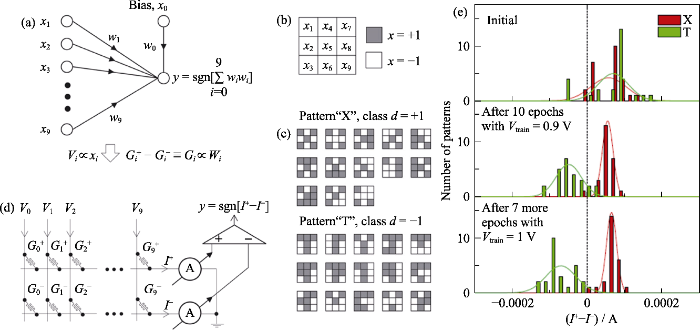
图1
基于TiO2-x忆阻器的单层感知器用于图像分类[74]
Fig. 1
Pattern classification using a single-layer perceptron based on TiO2-x memristor[74]
(a) Mathematical abstraction of the perceptron; (b) 3×3 binary images; (c) Two sets of images used for classification; (d) Memristive crossbar circuit for the perceptron; (e) Current difference histograms for 50 input images at different training epochs
1.1.2 双层氧化物结构
离子型忆阻器的阻变行为一般源于导电通道的形成与断裂, 随机性比较强, 这会导致器件与器件之间、器件不同开关周期的性能有较大差异[8]。合理组合的双层氧化物结构可以有效提升器件的稳定性和可靠性。此外, 双层氧化物忆阻器具有高度非线性, 有利于器件高密度集成。
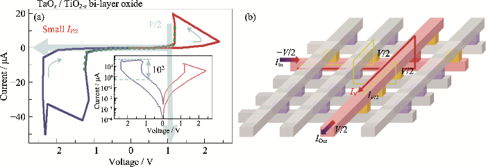
Pt/TaOx/TiO2-x/Pt忆阻器[75]表现出高度非线性的电流-电压特性, 如图2(a)所示。器件电流-电压的高度非线性有利于最大限度地减少交叉阵列的串扰电流, 这里非线性是指施加V/2电压时器件电流的变化情况(V为写电压)[75]。基于常用的电寻址方法, 对阵列中需要读写的忆阻器两端电极分别施加V/2和-V/2的电压, 这样器件的总压降是V, 如图2(b)中的红色器件。与其共享电极的同行或同列器件, 压降为V/2, 称为半选择器件, 如图2(b)中的黄色器件。这些半选择或者其它未选择器件中流过的电流称为串扰电流, 如图2(b)中黄线电流。串扰电流会使驱动电路饱和, 并产生多余的焦耳热, 从而限制阵列的实际应用尺寸。另外, 串扰电流引起的背景信号还会限制读取操作, 尤其在高电导态。非线性TaOx/TiO2-x双层氧化物忆阻器在施压V/2时电流小于1 μA, 基于其集成的交叉阵列规模可达1000行/列[75]。
图2
Choi等[76]制备了Ti/TaOx/HfO2/Pt双极性忆阻器, 其中HfO2和TaOx分别利用原子层沉积和溅射法制备。不同制备方法造成的物理缺陷的差异以及Ti电极的氧储备能力, 使得TaOx层比HfO2层具有更多的氧空位。导电通道的形成和断裂发生在连接最脆弱的TaOx/HfO2界面。TaOx层的插入有目的地改变了氧空位浓度, 实现了对导电通道的有效控制, 使得器件的工作状态更稳定、更可靠。在相同的电压脉冲激励下, 随着脉冲数量的增加, 器件的电导态表现出线性、对称的多态变化。基于这一阻变特性, 器件可以模拟大脑突触的增强、抑制功能和脉冲时间依赖可塑性学习规则。
BiFeO3器件具有大开关比, HfO2器件具有速度快、能耗低、多阻态等优点。基于这两种氧化物制备的Pt/BiFeO3/HfO2/TiN忆阻器[77], 其存储窗口(高低阻态的电阻之比)可达104, 测试寿命可达108脉冲周期, 通过施加不同的终止电压可实现多阻态变化。BiFeO3/HfO2结构中, HfO2是开关层, BiFeO3是富氧层, 为氧化还原反应提供氧离子, 从而显著延长了器件寿命。电形成初始化后, 器件的TiN电极附近聚集了较多氧空位, 形成了导电通道; 在随后的Reset过程中, 组成导电通道的部分氧空位发生还原反应, 剩余的氧离子聚集在HfO2/TiN界面形成肖特基势垒, 并且势垒高度随着负压增加而增大。
双层氧化物有利于提升器件的工作性能, 因此双层氧化物忆阻器得到了广泛研究, 例如Ta2O5-x/ TaO2-x[78]、HfO2/TiOx[79]、HfOx/HfOy[80]、TaOx/AlOy[81]、AlOx/NbOy[82]、ZnO/MgO[83]、InGaZnOx/InGaZnOy[84]、CeO2/Sn掺杂In2O3[85]、HfAlOx/TaOy[86]、ZnO/SiOx[87]、Sr2IrO4/BaTiO3[88]、TaOx/InGaZnO[89]、HfO2/Al2O3[90]、TaOx/ZnO[91]、AlOx/AlOy[92]、AlOx/ZnO[93]、InGaZnOx/N掺杂InGaZnOy[94]等等。
1.1.3 氧化物/其它材料混合结构
基于过渡金属氧化物和硫化物(MoOx/MoS2和WOx/WS2)制备的双极性忆阻器[97], 工作电压不高于0.2 V, 开关比可达106。在电压激励下, 电极/氧化物界面的肖特基势垒因为氧离子迁移发生改变, 进而对器件电导态实现多级调控。
Zhao等[98]在顶电极和忆阻层之间插入了石墨烯量子点(Graphene quantum dots, GQDs), 制备了Pt/GQDs/FeOx/Pt结构的忆阻器。其中, GQDs可以释放大量氧离子, 充当器件的纳米蓄氧池。使用GQDs将阻态分布的不稳定性降低了85%, 将开关电压及其分布范围分别降低和缩小了40%和84%。
在实际应用中, 读取操作的频率要远高于写入和擦除操作, 因此, 无功耗读写功能将进一步降低器件能耗。基于WOx/OAC(Oxygen-plasma-treated amorphous carbon, 氧等离子体处理非晶碳)制备的湿气供电忆阻器[99], 可以通过呼吸读取器件的开路电压, 与器件的电导态相对应。其中, WOx为忆阻层, OAC为纳米发电机。在电压驱动下, 氧离子在WOx/OAC界面发生迁移, 使器件的电导态和开路电压同时发生改变。
1.2 金属离子迁移型
1.2.1 单层氧化物结构
Tsunoda等[107]制备了Ag/TiO2/Pt结构忆阻器, 将其开关电压分别设置为0.5 V和-0.2 V, 可实现双极性开关模式。在Set过程中, Ag电极发生氧化反应, 产生的Ag离子在TiO2层中扩散, 到达Pt电极后发生还原反应, 形成由Ag原子组成的导电通道, 器件电导增大。在Reset过程中, 导电通道在焦耳热和反向电场的共同作用下发生断裂, 器件电导减小。
图3
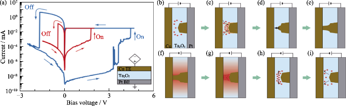
Valov等[109]揭示了非晶态TaOx样品的微观阻变机理。以Ta为底电极, 通过扫描隧道显微镜的探针针尖向样品施加负电压, TaOx中的Ta离子会向针尖移动, 发生还原反应, 在针尖和TaOx之间建立金属量子点接触, 样品电导升高; 移除电场后, 金属点接触会维持一段时间, 然后断开, 样品电导降低。
Ta/HfO2/Pt结构忆阻器[110]的阻态变化也是由金属离子迁移引起。器件的开关速度小于5 ns, 寿命超过1011个读写周期, 可以获得24个稳定电导态。器件的Ta和Pt分别为顶电极和底电极。在电形成初始化和Set过程中, 施加正电压, Ta氧化为Tax+, 在电场和离子浓度差作用下, Tax+向HfO2层迁移, O2-被牵引到Ta电极, 器件电导升高。通过扫描透射电镜可以在HfO2层中观察到直径小于10 nm富含Ta的圆锥状导电通道。在Reset过程中, 施加负电压, 钽离子被拽回Ta电极, 氧离子被推向Pt电极, 器件电导降低。
1.2.2 双层氧化物结构
Wang等[114]制备了Ag/SiO2/Ta2O5/Pt双层氧化物结构忆阻器, 其中SiO2层控制Ag通道的形状和生长方向, 1.5 nm超薄的Ta2O5层控制导电通道的形成和断裂。器件的工作电压小于0.3 V, 性能稳定。在1000次开关过程中, Set电压分布范围小于0.1 V, Reset电压分布范围小于0.08 V。而Ag/Ta2O5/SiO2/Pt结构忆阻器, 经500次开关操作后便被硬击穿了。
相反的氧化物堆叠顺序会使器件具有不同极性的开关模式, 如Ag/SnO2/InGaZnO (IGZO)/Pt和Ag/ IGZO/SnO2/Pt结构忆阻器[115], 前者为双极性, 后者为单极性。对于SnO2/IGZO结构器件, Ag导电通道断裂发生在IGZO/Pt界面, Ag离子的迁移速度和氧化还原反应速率较快, 器件的工作电压较低; 而对于IGZO/SnO2结构器件, Ag导电通道断裂发生在IGZO/SnO2界面, Ag离子的迁移速度和氧化还原反应速率较慢, Reset过程起主要作用的是焦耳热, 器件的工作电压较高。
Ag/Fe3O4/Ta2O5/Pt和Ag/Ta2O5/Fe3O4/Pt结构忆阻器[116]相比较, 两者均为双极性工作模式, 前者的电形成初始化电压更低,工作性能更好。Fe3O4/Ta2O5结构开关寿命较长, 能耗较低, 这是因为在Reset过程中, Ag导电通道断裂主要发生在Fe3O4层, 有效抑制了后续Set过程中导电通道扩大, 从而避免了器件在测试过程中被永久性击穿。
Pt/LiCoO2/SiO2/Si结构忆阻器[117]中, LiCoO2为Li离子源和阻变层, SiO2为Li离子捕获层。电压脉冲施加在Pt顶电极, Si衬底接地。当对器件施加正电压时, Li离子脱离LiCoO2, 穿过SiO2, 最终到达Si衬底, 形成LixSi, 器件电导升高, 对应Set过程, 反之, 对应Reset过程。Li离子在LiCoO2中均匀分布, 而Li离子在非晶态SiO2中的嵌入过程是非均匀的, 只发生在部分区域, 因此基于单层氧化物LiCoO2忆阻器的电导态是逐渐变化的, 而基于双层氧化物LiCoO2/SiO2器件的电导态是突变的, 并且SiO2层的厚度对器件电导态有显著影响。
此外, Giapintzakis等[118]制备了基于LiCoO2/ SiOx/TiO2的三层氧化物忆阻器, 其中LiCoO2为阻变阴极层, SiOx为电解质, TiO2为阳极层。对器件施加负电压时, Li+离子脱离LiCoO2, 穿过SiOx层向TiOx迁移, 器件电导升高; 反之, Li+离子返回LiCoO2, 器件电导降低。由于纳米电池效应, 器件有着非对称的类似于二极管的电流-电压特征, 使得器件能够像生物突触一样进行单向信号传输。三层氧化物忆阻器还有Ag/Zr0.5Hf0.5O2 (ZHO)/氧化石墨烯量子点(GOQDs)/ZHO/Pt[119]、Ag/ZHO/GOQDs/ZHO/Ag[119]等, 分别具有突变和连续变化的阻变特性。
1.2.3 氧化物/其它材料混合结构
Hwang等[120]制备了Cu/Cu2-xS/WO3-x/W结构忆阻器, 其中WO3-x为忆阻层, Cu2-xS为类似于二极管的分压器。使用两个该忆阻器和一个晶体管组成的突触器件可双向可逆调控电导[121]。在 HfO2和Cu2S之间插入Ta层可有效控制Cu离子扩散, 得到性能稳定的Cu/HfO2/Ta/Cu2S/W忆阻器[122]。将该忆阻器用作神经形态突触, 可有效提升神经网络的分类精度。Yan等[123]利用有序排列的PbS量子点控制Ag/Ga2O3/PbS QDs/Pt忆阻器中Ag+通道的生长, 降低了器件的阈值电压和能耗, 提升了器件开关电压分布的均匀性和电导态的保持特性, 并提高了器件的开关速度。通过控制金属离子导电通道生长, 提升器件工作性能的忆阻器结构还有TiN/HfAlOx[124]、ZnO/Ag[125]、ZrO2/WS2[126]、LiCoO2/a-Si[127]等。
1.3 纯电子型
氧离子型和金属离子型忆阻器的阻变机理涉及化学反应, 纯电子型忆阻器只涉及物理变化。纯电子型器件的阻变源于材料缺陷对电子的捕获和释放, 一方面表现为器件的整体行为, 另一方面不涉及微结构变化, 因此器件工作性能稳定, 器件之间重复性较好。
TiN/Ta2O5/Ta结构忆阻器[130]的整流比(+1 V和-1 V时高电导态电流之比)可达104, 有利于抑制器件阵列的串扰电流。其阻变来自电子在Ta2O5/Ta界面的捕获与释放。在TiN底电极和Ta2O5之间插入约4 nm厚的HfO2层, 会阻碍电子捕获及释放, 从而显著减小滞回电流。
Ag/Al2O3/GQDs/Al2O3/ITO结构的电子型突触器件[131], 其功能等效于忆阻器和电容并联。对器件施加首个正电压脉冲, 电子通过Fowler-Nordheim隧穿效应由Ag电极注入到Al2O3/GQDs/Al2O3结构, 器件达到最大电导。部分注入电子被GQDs/Al2O3界面捕获, 形成内部电场, 削弱GQDs和Ag电极之间的外部电场, 抑制电子注入, 从而降低器件电导。对器件施加首个负脉冲, 之前捕获的电子被释放, 器件电导恢复到较高的状态。后续负脉冲激发的部分注入电子被Al2O3/GQDs界面捕获, 器件电导降低。Al2O3厚度的精准控制和GQDs的均匀分布使器件成品率>95%, 器件性能稳定, 功耗低。基于Au@Al2O3壳核纳米颗粒的突触器件[132]也具有类似的工作性能。
双极性Pt/Al2O3/Si3N3.0/Ti忆阻器[133]的阻变来自Si3N3.0层均匀分布的缺陷对电子的捕获和释放。Al2O3为界面势垒层, 用于阻碍电子从Pt电极注入, 实现器件的自整流功能。对器件施加正向电压, 低电导态时, Poole-Frenkel导电机制占主导地位; 高电导态时, Fowler-Nordheim隧穿效应占主导地位。
2 光电混合调控忆阻器
光电混合调控忆阻器用电信号和光信号共同参与电导态调控, 根据阻变机理可分为离子型和纯电子型。
2.1 离子迁移型
ZnO-Au核壳纳米棒结构光电忆阻器[134]的阻变源于氧空位导电通道在正负电压脉冲作用下的形成和断裂。黑暗环境中施加电压脉冲, 器件不表现阻变特性。在300 W氙灯照射下, 器件表现出明显的电控双极性突变型阻变特性。光照能够调节ZnO界面氧离子的吸附数量, 使ZnO界面像一个蓄氧池, 通过控制光功率密度可调控器件的开关比和阻值大小。
Pd/MoOx/ITO结构光电忆阻器[136]的Set过程可以用365 nm紫外光进行调控, Reset过程可以用电信号进行调控。当紫外光照射ITO顶电极时, MoOx层中的光生电子进入导带, 光生空穴和吸收的水分子发生反应, 产生质子, Mo6+转变为Mo5+, 生成HyMoOx, 器件电导升高。其后, 对器件施加负电压, 质子向Pd电极漂移, Mo5+变回Mo6+, 器件电导减小。该器件能够存储光照信息并实现光可调突触功能。
2.2 纯电子型
水热法制备的ZnO纳米棒/铌掺杂SrTiO3(NSTO)异质结忆阻器[137], 可通过调整正负电压脉冲的幅值, 实现多电导态变化。紫外光照射可使器件在一个较高的电导状态持续工作, 退火处理才能使其恢复到初始状态。该持续光电导现象是由光照产生的空穴和电离氧空位在ZnO/NSTO界面聚集引起。空穴和电离氧空位有效质量大, 迁移率低, 漂移回原状态的速度慢, 因此寿命较长。
ITO/ZnO1-x/AlOy/Al结构忆阻器[138]在黑暗环境和310 nm紫外光照射下具有相似的阻变特性。器件高电导态的保持特性优异, 而低电导态的保持性较差。光照使器件电流持续升高, 光照停止后, 器件电流逐渐衰减, 表现出持续光电导现象。这种现象产生机理如下: 当对器件施加光照时, 电子被激发到导带, 电导升高, 光生空穴聚集在ZnO1-x/AlOy界面, 并在内建电场作用下被AlOy层捕获; 光照撤除后, 光生空穴会有一定概率越过界面势垒回到原处, 从而产生持续光电导效应。通过调整光照频率, 该器件可模拟神经突触的长程和短程可塑性功能。
3 全光控忆阻器
Zhuge等[34]基于缺氧InGaZnO/富氧InGaZnO(OD- IGZO/OR-IGZO)同质结, 首次实现了全光控忆阻器。OD-IGZO/OR-IGZO器件的光电响应波长大于1000 nm, 其独特的长波长响应特性是实现全光可逆调控的基础。在可见光(420~650 nm)和近红外光(800~1000 nm)照射下, 器件由初始低电导态变为非易失的高电导态, 表现出明显的持续光电导现象, 如图4(a)所示。光Set机理为: 光照使OD-IGZO/OR- IGZO界面的中性氧空位电离, 电离氧空位浓度增大, 界面势垒宽度减小, 器件电导升高。Reset过程使用的光波长在很大程度上取决于Set光波长, Set光波长越短, 后续光Reset效果越好。光Reset机理为: 长波光照射下, OD-IGZO/OR-IGZO界面势阱中的电子被激发到势垒区, 被电离氧空位俘获, 电离氧空位浓度减小, 界面势垒宽度增大, 器件电导降低。如图4(b)所示, Set过程使用420 nm的蓝光照射15 s, 10 min之后分别使用绿光(530 nm)、红光(650 nm)和近红外光(800和900 nm)照射, 发现近红外光照射可以使器件电流大幅下降, 对应Reset过程, 其中800 nm光照下Reset效率更高。如果Set和Reset过程分别使用420 nm蓝光和800 nm近红外光, 器件可以表现出稳定的开关特性和状态保持特性, 并可模拟突触的脉冲时间依赖可塑性学习规则。图4(c)为脉冲时间依赖可塑性规则的突触增强模拟过程: 首先, 将器件的电导调整到一个相对低的状态Mc0≈100 nS; 然后, 用蓝光脉冲照射, 器件电导升高; 接着, 在间隔Δt1和Δt2(Δt2>Δt1>0)后用近红外光脉冲照射, 器件电导变为Mc1和Mc2(Mc1>Mc2>Mc0)。图4(d)为脉冲时间依赖可塑性规则的突触抑制模拟过程: 首先, 将器件的电导调整到一个相对高的状态Mc0≈250 nS; 然后, 用近红外光脉冲照射, 器件电导降低; 接着, 在间隔Δt1和Δt2(Δt2<Δt1<0)后用蓝光脉冲照射, 器件电导变为Mc1和Mc2(Mc1<Mc2<Mc0)。
图4
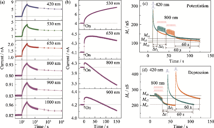
图4
OD-IGZO/OR-IGZO全光控忆阻器[34]
Fig. 4
All-optically controlled memristor based on OD-IGZO/OR-IGZO[34]
(a) Optical Set behavior upon irradiation with light of various wavelengths; (b) Photocurrent responses to irradiation with light of various wavelengths after blue light irradiation; (c) Synaptic potentiation process of spike-timing dependent plasticity;(d) Synaptic depression process of spike-timing dependent plasticity
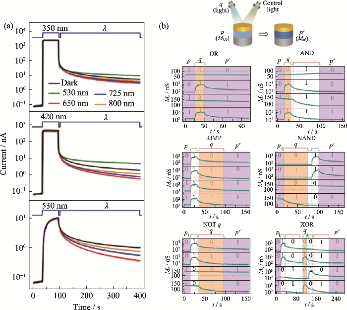
Zhuge等[35]进一步制备了简单的Au/ZnO/Pt结构全光控忆阻器, 研究发现, 整个ZnO薄膜都位于肖特基势垒区, 其阻变来自不同波长光照下氧空位的电离和中和, 导致ZnO导带底曲率增大和减小。350、420和530 nm的短波光照射使器件电导升高, 对应光Set过程; 而650、725和800 nm的长波光照射对器件几乎没有影响。如果先用350和420 nm光照射器件, 随后分别用530、650、725和800 nm光照射器件, 和无后续光照情况相比, 530 nm光照升高器件电导, 而650、725和800 nm光照降低器件电导, 即发生Reset。如果先用530 nm光照射器件, 再用长波光照射器件, 也能发生Reset, 如图5(a)所示。Set和Reset分别使用530 nm绿光和650 nm红光, 器件表现出稳定的阻变特性和优良的电导态保持特性。将该器件的测试数据用作突触权重, 基于CrossSim搭建的三层神经网络可识别8×8和28×28像素的手写数字, 并且在3次迭代后准确率达到了92%。该器件也可用于实现全部16种布尔逻辑运算功能, 并将结果以电导态的形式原位存储, 如图5(b)所示。其中, p和p′分别表示器件的初始和最终电导态(电导值大于100 nS取1, 反之取0), q表示530或650 nm光照(有、无光照分别取1和0); p和q为输入, p′为输出。以“AND”运算为例: q为530 nm光照, 之后统一采用650 nm控制光照; (1)p=0(低电导态), q=0(无530 nm光照), 650 nm控制光照对器件无显著影响, 输出p′=0; (2)p=0, q=1(530 nm光照射, 将器件从低电导态转换到高电导态), 之后用650 nm控制光照, 将器件从高电导态转变回低电导态, 输出p′=0; (3)p=1(高电导态), q=0, 之后用650 nm控制光照, 将器件从高电导态转换到低电导态, 输出p′=0; (4)p=1, q=1(530 nm光照射, 将器件调整到更高电导态), 之后用650 nm控制光照, 器件仍然处于高电导态, 输出p′=1。
图5
基于Ag-TiO2复合纳米材料制备的全光控忆阻器[141], 其Set和Reset过程分别使用可见光和紫外光照射。可见光照射下, 在银纳米颗粒的表面局域等离子激元效应作用下, 热电子被激发到TiO2导带, 银颗粒发生光氧化, Ag/TiO2微纳界面的肖特基势垒减弱, 器件电导升高。紫外光照射下, TiO2价带电子被激发到导带, 与Ag离子复合, 器件电导减小。
4 结束语
大部分电控氧化物忆阻器的阻变源于氧离子或金属离子组成的纳米级导电通道的形成和断裂, 随机性强, 使得器件与器件之间、器件在不同的开关周期工作性能差异较大, 不利于器件的大规模集成。双层氧化物和氧化物与其它材料的复合能有效控制离子迁移, 从而提升器件的稳定性和可靠性。与离子迁移型忆阻器相比, 纯电子型器件表现为整体阻变行为, 并且不涉及微结构变化, 因此性能有望更稳定可靠。
氧化物忆阻器自1962年[142]被首次报道以来,取得了显著进步, 例如, 器件尺寸已小至2 nm[14]; 开关速度可小于100 ps[143]; 开关比可达106[97]; 器件寿命超过1012个开关周期[78]; 器件单脉冲能耗低至4.28 aJ[15], 甚至小于人脑的单脉冲能耗(根据人脑功耗10 W推算, 单次突触行为能耗小于10 fJ[144])。不过, 这些特性并没有集中在单个器件上, 以氧化物忆阻器为突触的神经形态网络已实现部分人脑功能, 如图像处理、识别、分类[24⇓⇓⇓-28]和联想记忆[86]等。但是, 目前用于神经网络的忆阻器阵列还不够大, 主要原因有: 器件性能不一致, 不利于集成和应用; 缺少理想的开关选择器, 现有的很多阵列使用晶体管作为开关元件, 一个忆阻器需要一个晶体管, 严重限制了阵列密度。另外, 基于氧化物忆阻器的人工突触主要应用于普通人工神经网络, 而脉冲神经网络研究甚少。后者以脉冲时间依赖可塑性学习规则为基础, 信息处理方式更接近人脑[68]。
和电信号相比, 光信号速度超快、带宽大, 用于调控电导态, 不仅能有效降低能耗, 而且能避免焦耳热的产生和微结构变化[34,139,145]。此外, 光电忆阻器可直接感受外界光信号, 实现感/存/算一体, 从而大幅提升人工视觉系统的效率[139]。由于半导体材料固有的光电效应, 光照一般只能增大器件电导[137-138], 或者通过熔断之前利用电刺激形成的导电通道来降低器件电导[135], 因此, 实现全光控忆阻器[34]是忆阻器发展历史上的一大突破。但是, 光照下氧化物忆阻器电导态变化的微观机理还不够清晰, 难以精准调控电导态; 尤其是全光控忆阻器, 其光致电导降低的确切机理, 仍然需要进一步合理阐释。另外, 光电忆阻器光信号的引入方式又决定了器件的集成规模。
由于在类脑计算领域的应用前景广阔, 氧化物忆阻器正吸引着越来越多研究者的关注。自2000年以来, 众多半导体公司也布局了这一新兴领域。未来氧化物忆阻器的发展, 亟需多领域交叉合作, 包括物理、材料、微电子、光电子、计算机、神经科学等。相信在不久的将来, 基于氧化物忆阻器的类脑计算芯片将能满足人类社会对海量信息的实时处理需求。
参考文献
Emerging artificial neuron devices for probabilistic computing
Neuromorphic electronic systems
A million spiking-neuron integrated circuit with a scalable communication network and interface

\n Computers are nowhere near as versatile as our own brains. Merolla\n et al.\n applied our present knowledge of the structure and function of the brain to design a new computer chip that uses the same wiring rules and architecture. The flexible, scalable chip operated efficiently in real time, while using very little power.\n
A single-transistor silicon synapse
Parallel programming of an ionic floating-gate memory array for scalable neuromorphic computing
Neuromorphic computers could overcome efficiency bottlenecks inherent to conventional computing through parallel programming and readout of artificial neural network weights in a crossbar memory array. However, selective and linear weight updates and <10-nanoampere read currents are required for learning that surpasses conventional computing efficiency. We introduce an ionic floating-gate memory array based on a polymer redox transistor connected to a conductive-bridge memory (CBM). Selective and linear programming of a redox transistor array is executed in parallel by overcoming the bridging threshold voltage of the CBMs. Synaptic weight readout with currents <10 nanoamperes is achieved by diluting the conductive polymer with an insulator to decrease the conductance. The redox transistors endure >1 billion write-read operations and support >1-megahertz write-read frequencies.Copyright © 2019 The Authors, some rights reserved; exclusive licensee American Association for the Advancement of Science. No claim to original U.S. Government Works.
Fully memristive neural networks for pattern classification with unsupervised learning
Memristive synapses for brain-inspired computing
Toward a generalized Bienenstock- Cooper-Munro rule for spatiotemporal learning via triplet-STDP in memristive devices
Spin-orbit torque induced spike-timing dependent plasticity
Nanoelectronic devices that mimic the functionality of synapses are a crucial requirement for performing cortical simulations of the brain. In this work, we propose a ferromagnet-heavy metal heterostructure that employs spin-orbit torque to implement spike-timing dependent plasticity. The proposed device offers the advantage of decoupled spike transmission and programming current paths, thereby leading to reliable operation during online learning. Possible arrangement of such devices in a crosspoint architecture can pave the way for ultra-dense neural networks. Simulation studies indicate that the device has the potential of achieving pico-Joule level energy consumption (maximum 2 pJ per synaptic event) which is comparable to the energy consumption for synaptic events in biological synapses.
Memristor-the missing circuit element
Resistance switching memories are memristors
The missing memristor found
Memristor crossbar arrays with 6-nm half-pitch and 2-nm critical dimension
Three-dimensional nanoscale flexible memristor networks with ultralow power for information transmission and processing application
Photoelectric memristor-based machine vision for artificial intelligence applications
Spike-enabled audio learning in multilevel synaptic memristor array-based spiking neural network
A braitenberg vehicle based on memristive neuromorphic circuits
Memristor-based biomimetic compound eye for real-time collision detection
Experimental demonstration of highly reliable dynamic memristor for artificial neuron and neuromorphic computing
Neural signal analysis with memristor arrays towards high-efficiency brain-machine interfaces
Training and operation of an integrated neuromorphic network based on metal-oxide memristors
Sparse coding with memristor networks
Memristor-based analog computation and neural network classification with a dot product engine
Face classification using electronic synapses
Fully hardware-implemented memristor convolution neural network
Mechanism for resistive switching in chalcogenide-based electrochemical metallization memory cells
It has been reported that in chalcogenide-based electrochemical metallization (ECM) memory cells (e.g., As2S3:Ag, GeS:Cu, and Ag2S), the metal filament grows from the cathode (e.g., Pt and W) towards the anode (e.g., Cu and Ag), whereas filament growth along the opposite direction has been observed in oxide-based ECM cells (e.g., ZnO, ZrO2, and SiO2). The growth direction difference has been ascribed to a high ion diffusion coefficient in chalcogenides in comparison with oxides. In this paper, upon analysis of OFF state I–V characteristics of ZnS-based ECM cells, we find that the metal filament grows from the anode towards the cathode and the filament rupture and rejuvenation occur at the cathodic interface, similar to the case of oxide-based ECM cells. It is inferred that in ECM cells based on the chalcogenides such as As2S3:Ag, GeS:Cu, and Ag2S, the filament growth from the cathode towards the anode is due to the existence of an abundance of ready-made mobile metal ions in the chalcogenides rather than to the high ion diffusion coefficient.
Artificial synapse emulated by charge trapping-based resistive switching device
Nonvolatile resistive switching memory based on amorphous carbon
Resistive memory effect has been found in carbon nanostructure-based devices by Standley et al. [Nano Lett. 8, 3345 (2008)]. Compared to nanostructures, hydrogenated amorphous carbon (a-C:H) has much more controllable preparation processes. Study on a-C:H-based memory is of great significance to applications of carbon-based electronic devices. We observed nonvolatile resistance memory behaviors in metal/a-C:H/Pt structures with device yield 90%, ON/OFF ratio &gt;100, and retention time &gt;105 s. Detailed analysis indicates that the resistive switching originates from the formation/rupture of metal filaments due to the diffusion of the top electrodes under a bias voltage.
Mechanism of nonvolatile resistive switching in graphene oxide thin films
Single-crystalline metal filament- based resistive switching in a nitrogen-doped carbon film containing conical nanopores
In this letter, we report on the resistive switching originating from the rupture/rejuvenation of single-crystalline Cu filaments in a nitrogen-doped porous carbon-based memristive device Cu/CN0.15/Pt. Cu filaments are confined in conical nanopores in CN0.15 thin films. Dislocations exist in the Cu filaments, resulting in obvious crystal lattice distortions. The Cu/CN0.15/Pt device shows outstanding high temperature retention performance for both ON and OFF states, indicating that it is promising for resistance memory applications. Furthermore, continuous RESET (ON-to-OFF switching) and SET (OFF-to-ON switching) processes could be realized indicating the adaptive learning ability of Cu/CN0.15/Pt, which has potential applications in synaptic devices.
All-optically controlled memristor for optoelectronic neuromorphic computing
Optically driven intelligent computing with ZnO memristor
Direct identification of the conducting channels in a functioning memristive device
Atomic structure of conducting nanofilaments in TiO2 resistive switching memory
Unipolar resistive switching characteristics of room temperature grown SnO2 thin films
The resistive switching characteristics of room temperature grown SnO2 films were investigated by fabricating the metal-oxide-metal sandwich structures. The unipolar operation was found in all devices. Experiments, including the size and material dependencies of the top electrodes and the three terminal device structures, demonstrated the rupture and formation of conducting filaments near the anode. The Ohmic behavior was observed in both on- and off-states when using Au and Ti top electrodes, whereas the Schottky behavior was only found in the off-state for Pt. The analysis on the transport properties indicates the presence of insulative crystalline SnO2 near the anode in the off-state.
Forming free colossal resistive switching effect in rare-earth-oxide Gd2O3 films for memristor applications
The reproducible forming-free resistive switching (RS) behavior in rare-earth-oxide Gd2O3 polycrystalline thin film was demonstrated. The characteristic of this forming-free RS was similar to that of other forming-necessary binary RS materials except that its initial resistance starts from not the high resistance state (HRS) but the low resistance state (LRS). An ultrahigh resistance switching ratio from HRS to LRS of about six to seven orders of magnitude was achieved at a bias voltage of 0.6 V. Mechanism analysis indicated that the existence of metallic Gd in the Gd2O3 films plays an important role in the forming-free RS performance. Our work provides a novel material with interesting RS behavior, which is beneficial to deepen our understanding of the origin of RS phenomenon.
Resistive switching in CeOx films for nonvolatile memory application
Nonpolar resistive switching in the Pt/MgO/Pt nonvolatile memory device
Nonpolar resistive switching (RS), which is the coexistence of unipolar and bipolar RS characteristics, in the Pt/MgO/Pt memory device with the nonforming nature is demonstrated. The nonforming nature is ascribed to the relatively high defect density of the MgO film deposited by using the ion beam sputtering in Ar atmosphere. The results of Auger electron spectroscopy and x-ray photoelectron spectroscopy analyses combing with the temperature dependence of resistance suggest that metallic Mg filaments are formed in the low resistance state. The voltage-polarity-independent RESET process implies that filaments may be ruptured by local Joule heating, leading to nonpolar characteristics.
Ionic doping effect in ZrO2 resistive switching memory
Oxygen vacancy (VO) plays the critical role for resistive switching in transition metal oxide resistive random access memory (RRAM). First principles calculation is performed to study the impact of metallic ion (Al, Ti, or La) doping in ZrO2 on the behaviors of VO, including defect energy level and formation energy (Evf). Trivalent dopant (Al or La) significantly reduces Evf. Based on the calculated results, ZrO2-based RRAM devices are designed to control the formation of VO, and improved resistive switching uniformity is demonstrated in experiments.
Unipolar switching behaviors of RTO WOx RAM
Resistive switching characteristics of TiN/MnO2/Pt memory devices
Effect of top electrode materials on bipolar resistive switching behavior of gallium oxide films
Well-developed bipolar resistive switching behaviors have been revealed in Pt/GaOx/ITO stacks without an electroforming process. By substituting platinum with titanium as the top electrode, switching polarity changed from “counter-Figure-8” to “Figure-8.” The modulation of Schottky barrier at the Pt/GaOx interface induced by migration of oxygen vacancies was proposed to explain the switching in Pt/GaOx/ITO stacks, while the switching in Ti/GaOx/ITO stacks was ascribed to the redox reaction at the Ti/GaOx interface. Our experimental result further confirms the migration of oxygen vacancies in the vicinity of the electrode area plays an important role in the resistive switching process.
Bipolar resistive switching in heterostructures: bismuth oxide/normal metal
Bipolar resistive switching of chromium oxide for resistive random access memory
Intrinsic resistive switching and memory effects in silicon oxide
Optical, electrical properties and reproducible resistance switching of GeO2 thin films by Sol-Gel process
Resistive switching properties of molybdenum oxide films
Concurrent presence of unipolar and bipolar resistive switching phenomena in pnictogen oxide Sb2O5 films
The concurrent presence of unipolar resistive switching (URS) and bipolar resistive switching (BRS) characteristics of the Sb/Sb2O5/Pt structure were examined. It was discovered that the BRS phenomenon was driven by the abnormal reset process during URS cycles which was induced by the rupture and recovery of the conducting filament (CF) in the localized region near the anode. The electrical conduction behavior in the high resistance state of URS and BRS was explained by the Schottky emission and space-charge-limited current mechanism, meaning that the URS and BRS phenomena are induced by the extent of reoxidaton and reduction regarding the local CF-ruptured region.
Unipolar memristive switching in yttrium oxide and RESET current reduction using a yttrium interlayer
Resistive switching mechanisms relating to oxygen vacancies migration in both interfaces in Ti/HfOx/Pt memory devices
Resistive switching mechanism of Ti/HfOx/Pt memory devices was studied using X-ray photoelectron spectroscopy and cross-sectional transmission electron microscopy images. Spatial distributions of valence of Hf demonstrated that the fraction of Hf4+ increased from Ti/HfOx interface to HfOx/Pt interface in high resistance state (HRS), but it maintained a constant level in low resistance state (LRS). Rupture of oxygen vacancies formed conducting paths occurred near the HfOx/Pt interface. The cross sectional images of active switching region also varied with HRS and LRS. A dynamic model of interface processes was proposed to interpret interfaces migration of oxygen vacancies near both the top and bottom electrodes.
Coexistence of unipolar and bipolar resistive switching in Pt/NiO/Pt
We demonstrate the coexistence of unipolar and bipolar resistive switching in NiO thin film fabricated by reactive sputtering. It was shown that the required voltages for switching operations in the bipolar switching mode are smaller than the voltages in the unipolar mode, while the ON/OFF resistance levels are similar for the two modes. The NiO resistive switching device also exhibited transitions between the two switching modes, with the subsequent I-V characteristics unaffected by the switching history, which clearly indicates that the two switching mechanisms are directly related. The switching versatility in NiO is expected to facilitate improved device performance, for example, by increasing the margin of programming voltages. Based on the investigation of device characteristics, we discuss the switching processes for the two switching modes and their relationship.
Annealing effect on the bipolar resistive switching behaviors of BiFeO3 thin films on LaNiO3-buffered Si substrates
Redox-based resistive switching memories-nanoionic mechanisms, prospects, and challenges
Memristive devices for computing
Diffusion of adhesion layer metals controls nanoscale memristive switching
Memristive switching mechanism for metal/oxide/metal nanodevices
The mechanism of electroforming of metal oxide memristive switches
Metal/TiO2 interfaces for memristive switches
Coexistence of memristance and negative differential resistance in a nanoscale metal-oxide-metal system
Observation of two resistance switching modes in TiO2 memristive devices electroformed at low current
Memristive tri-stable resistive switching at ruptured conducting filaments of a Pt/TiO2/Pt cell
Interface-engineered amorphous TiO2-based resistive memory devices
High switching endurance in TaOx memristive devices
We demonstrate over 1×10¹⁰ open-loop switching cycles from a simple memristive device stack of Pt/TaOx/Ta. We compare this system to a similar device stack based on titanium oxides to obtain insight into the solid-state thermodynamic and kinetic factors that influence endurance in metal-oxide memristors.
Resistive switching in single epitaxial ZnO nanoislands
Resistive memory is one of the most promising candidates for next-generation nonvolatile memory technology due to its variety of advantages, such as simple structure and low-power consumption. Bipolar resistive switching behavior was observed in epitaxial ZnO nanoislands with base diameters and heights ranging around 30 and 40 nm, respectively. All four different states (initial, electroformed, ON, and OFF) of the nanoscale resistive memories were measured by conductive atomic force microscopy immediately after the voltage sweeping was performed. Auger electron spectroscopy and other experiments were also carried out to investigate the switching mechanism. The formation and rupture of conducting filaments induced by oxygen vacancy migration are responsible for the resistive switching behaviors of ZnO resistive memories at the nanoscale.
Learning of spatiotemporal patterns in a spiking neural network with resistive switching synapses
Resistive switching devices were used as technological synapses to learn about the spatial- and temporal-correlated neuron spikes.
Computing of temporal information in spiking neural networks with ReRAM synapses
Improving linearity by introducing Al in HfO2 as memristor synapse device
A memristor-based in-memory computing network for Hamming code error correction
Nitrogen-induced enhancement of synaptic weight reliability in titanium oxide-based resistive artificial synapse and demonstration of the reliability effect on the neuromorphic system
Improvement of resistive switching characteristics in zinc oxide-based resistive random access memory by ammoniation annealing
Pattern classification by memristive crossbar circuits using ex situ and in situ training
Engineering nonlinearity into memristors for passive crossbar applications
Although TaOx memristors have demonstrated encouraging write/erase endurance and nanosecond switching speeds, the linear current-voltage (I-V) characteristic in the low resistance state limits their applications in large passive crossbar arrays. We demonstrate here that a TiO2-x/TaOx oxide heterostructure incorporated into a 50 nm× 50 nm memristor displays a very large nonlinearity such that I(V/2) ≈ I(V)/100 for V ≈ 1 volt, which is caused by current-controlled negative differential resistance in the device.
Engineering synaptic characteristics of TaOx/HfO2 bi-layered resistive switching device
Designing high-performance storage in HfO2/BiFeO3 memristor for artificial synapse applications
A fast, high-endurance and scalable non-volatile memory device made from asymmetric Ta2O5-x/TaO2-x bilayer structures
An electronic synaptic device based on HfO2/TiOx bilayer structure memristor with self-compliance and deep-Reset characteristics
Adaptive crystallite kinetics in homogenous bilayer oxide memristor for emulating diverse synaptic plasticity
Bipolar analog memristors as artificial synapses for neuromorphic computing
Synaptic devices with bipolar analog resistive switching behavior are the building blocks for memristor-based neuromorphic computing. In this work, a fully complementary metal-oxide semiconductor (CMOS)-compatible, forming-free, and non-filamentary memristive device (Pd/Al2O3/TaOx/Ta) with bipolar analog switching behavior is reported as an artificial synapse for neuromorphic computing. Synaptic functions, including long-term potentiation/depression, paired-pulse facilitation (PPF), and spike-timing-dependent plasticity (STDP), are implemented based on this device; the switching energy is around 50 pJ per spike. Furthermore, for applications in artificial neural networks (ANN), determined target conductance states with little deviation (<1%) can be obtained with random initial states. However, the device shows non-linear conductance change characteristics, and a nearly linear conductance change behavior is obtained by optimizing the training scheme. Based on these results, the device is a promising emulator for biology synapses, which could be of great benefit to memristor-based neuromorphic computing.
Unsupervised Hebbian learning experimentally realized with analogue memristive crossbar arrays
A bio-inspired physically transient/biodegradable synapse for security neuromorphic computing based on memristors
Physically transient electronic devices that can disappear on demand have great application prospects in the field of information security, implantable biomedical systems, and environment friendly electronics. On the other hand, the memristor-based artificial synapse is a promising candidate for new generation neuromorphic computing systems in artificial intelligence applications. Therefore, a physically transient synapse based on memristors is highly desirable for security neuromorphic computing and bio-integrated systems. Here, this is the first presentation of fully degradable biomimetic synaptic devices based on a W/MgO/ZnO/Mo memristor on a silk protein substrate, which show remarkable information storage and synaptic characteristics including long-term potentiation (LTP), long-term depression (LTD) and spike timing dependent plasticity (STDP) behaviors. Moreover, to emulate the apoptotic process of biological neurons, the transient synapse devices can be dissolved completely in phosphate-buffered saline solution (PBS) or deionized (DI) water in 7 min. This work opens the route to security neuromorphic computing for smart security and defense electronic systems, as well as for neuro-medicine and implantable electronic systems.
Gradual switching and self-rectifying characteristics of Cu/α-IGZO/p+-Si RRAM for synaptic device application
A Pt/ITO/CeO2/Pt memristor with an analog, linear, symmetric, and long-term stable synaptic weight modulation
Analog synaptic weight modulation that is linear, symmetric, and exhibits long-term stability is demonstrated by the resistance changes in a Pt/indium-tin-oxide (ITO)/CeO2/Pt memristor. Distinct from a Pt/CeO2/Pt memristor without the ITO layer, which shows highly nonlinear and asymmetric resistance changes, the Pt/ITO/CeO2/Pt memristor exhibits linear and symmetric resistance changes in proportion to the number of voltage applications with opposite polarities for potentiation and depression behaviors. The Pt/CeO2/Pt memristor also displays high long-term stability of modulated synaptic weight over time, which originates from the ITO layer acting as a reservoir of oxygen ions drifted from the CeO2 layer to retain the resistance change. Comparison of the results for the Pt/CeO2/Pt and Pt/ITO/CeO2/Pt memristors confirms the role of ITO in the linearity, symmetry, and long-term stability of the resistance change in CeO2-based memristors for use as artificial synapses in neuromorphic systems.
Associative memory for image recovery with a high-performance memristor array
Bio-realistic synaptic characteristics in the cone-shaped ZnO memristive device
An epitaxial synaptic device made by a band-offset BaTiO3/Sr2IrO4 bilayer with high endurance and long retention
New types of artificial synaptic devices are important to develop highly reliable devices for high-intelligent neuromorphic information technologies. Here, we develop an epitaxial heterostructure with a small-gap spin-orbital-coupling-Mott insulator Sr2IrO4 and a large-gap ferroelectric BaTiO3 to implement robust artificial synapses. Electric-field-dependent synchrotron X-ray absorption spectroscopy indicates that oxygen vacancies are transferred to the bilayer surface by an applied voltage less than 5 V. Because of the epitaxial quality and the large band-gap offset, the prototype devices have robust bipolar-resistance-switching behaviors as demonstrated by the high endurance (&gt;104 cycles) and the long retention (&gt;104 s). The steady synaptic learning algorithm is made in the prototype device with multiple synaptic functions including the short term plasticity, long term plasticity, and spike timing dependent plasticity. Our study demonstrates the ferroelectric/spin-orbital-coupling-Mott oxide bilayer as a reliable prototype device that mimics the synapses in neural systems of the human brain.
Ar ion plasma surface modification on the heterostructured TaOx/InGaZnO thin films for flexible memristor synapse
Resistive switching and synaptic behaviors of an HfO2/Al2O3 stack on ITO for neuromorphic systems
Applications of p-n homojunction ZnO nanowires to one-diode one-memristor RRAM arrays
Forming-free, fast, uniform, and high endurance resistive switching from cryogenic to high temperatures in W/AlOx/Al2O3/Pt bilayer memristor
Memristive behavior enabled by amorphous-crystalline 2D oxide heterostructure
Resistive switching performance improvement of InGaZnO-based memory device by nitrogen plasma treatment
Low power forming free TiO2-x/Hf02-x/TiO2-x-trilayer RRAM devices exhibiting synaptic property characteristics
A low energy oxide-based electronic synaptic device for neuromorphic visual systems with tolerance to device variation
Layered memristive and memcapacitive switches for printable electronics
Novel computing technologies that imitate the principles of biological neural systems may offer low power consumption along with distinct cognitive and learning advantages. The development of reliable memristive devices capable of storing multiple states of information has opened up new applications such as neuromorphic circuits and adaptive systems. At the same time, the explosive growth of the printed electronics industry has expedited the search for advanced memory materials suitable for manufacturing flexible devices. Here, we demonstrate that solution-processed MoOx/MoS2 and WOx/WS2 heterostructures sandwiched between two printed silver electrodes exhibit an unprecedentedly large and tunable electrical resistance range from 10(2) to 10(8) Ω combined with low programming voltages of 0.1-0.2 V. The bipolar resistive switching, with a concurrent capacitive contribution, is governed by an ultrathin (<3 nm) oxide layer. With strong nonlinearity in switching dynamics, different mechanisms of synaptic plasticity are implemented by applying a sequence of electrical pulses.
Memristive devices with highly repeatable analog states boosted by graphene quantum dots
Moisture-powered memristor with interfacial oxygen migration for power-free reading of multiple memory states
Bipolar and unipolar resistive switching in Cu-doped SiO2
Impact of Cu electrode on switching behavior in a Cu/HfO2/Pt structure and resultant Cu ion diffusion
Resistive switching properties of Au/ZrO2/Ag structure for low-voltage nonvolatile memory applications
The resistive switching mechanism of Ag/SrTiO3/Pt memory cells
Nonvolatile multilevel memory effect in Cu/WO3/Pt device structures
Mechanism for resistive switching in an oxide-based electrochemical metallization memory
A comparison of the asymmetric OFF-state current-voltage characteristics between Cu/ZnO/Pt and Cu/ZnO/Al-doped ZnO (AZO) electrochemical metallization memory (ECM) cells demonstrates that the Cu filament rupture and rejuvenation occur at the ZnO/Pt (or AZO) interface, i.e., the cathodic interface. Therefore, the filament is most likely to have a conical shape, with wider and narrower diameters formed at the anodic and cathodic interfaces, respectively. It is inferred that the filament growth starts at the anode surface and stops at the cathode surface. Our results indicate that oxide-based ECM cells strongly differ from sulfide- and selenide-based ones in the resistive switching mechanism.
Nanobatteries in redox-based resistive switches require extension of memristor theory
Bipolar resistive switching in polycrystalline TiO2 films
Bipolar resistive switching was found in thin polycrystalline TiO2 films formed by the thermal oxidation of sputtered Ti films. With a Ag top electrode, TiO2 film, and Pt bottom electrode, bistable resistive switching with a low operating voltage and a good uniformity was observed repeatedly without an initial electrical “forming” process. This switching phenomenon might be described as the formation and rupture of a filamentary conductive path consisting of a chain of Ag atoms. The temperature dependence of the switching voltage is discussed in terms of interstitial ionic diffusion of Ag in the TiO2 matrix.
Forming and switching mechanisms of a cation-migration-based oxide resistive memory
Nanoscale cation motion in TaOx, HfOx and TiOx memristive systems
Sub-10 nm Ta channel responsible for superior performance of a HfO2 memristor
A CMOS-compatible electronic synapse device based on Cu/SiO2/W programmable metallization cells
Memristors with diffusive dynamics as synaptic emulators for neuromorphic computing
Design of defect- chemical properties and device performance in memristive systems
Impurities and dopants in memristive devices determine their switching kinetics, performance, and neuromorphic functionalities.
SiO2/Ta2O5 heterojunction ECM memristors: physical nature of their low voltage operation with high stability and uniformity
Dependence of InGaZnO and SnO2 thin film stacking sequence for the resistive switching characteristics of conductive bridge memory devices
Revealing conducting filament evolution in low power and high reliability Fe3O4/Ta2O5 bilayer RRAM
Lithium ion trapping mechanism of SiO2 in LiCoO2 based memristors
Evidence of biorealistic synaptic behavior in diffusive Li-based two- terminal resistive switching devices
Graphene oxide quantum dots based memristors with progressive conduction tuning for artificial synaptic learning
Improved synaptic behavior of CBRAM using internal voltage divider for neuromorphic systems
One transistor-two resistive RAM device for realizing bidirectional and analog neuromorphic synapse devices
Improved synapse device with MLC and conductance linearity using quantized conduction for neuromorphic systems
Self-assembled networked PbS distribution quantum dots for resistive switching and artificial synapse performance boost of memristors
Low-power artificial neurons based on Ag/TiN/HfAlOx/Pt threshold switching memristor for neuromorphic computing
Controllable digital resistive switching for artificial synapses and pavlovian learning algorithm
The fundamental unit of the nervous system is a synapse, which is involved in transmitting information between neurons as well as learning, memory, and forgetting processes. Two-terminal memristors can fulfil most of these requirements; however, their poor dynamic changes in resistance to input electric stimuli remain an obstacle, which must be improved for accurate and quick information processing. Herein, we demonstrate the synaptic properties of ZnO-based memristors, which were significantly enhanced (∼340 times) by geometrical modulation due to the localized electric field enhancement. Specifically, by inserting Ag-nanowires and Ag-dots into the ZnO/Si interface, the resistive switching could be controlled from a digital to analog mode. A finite element simulation revealed that the presence of Ag could enhance the localized electric field, which in turn improved the migration of ionic species. Further, the device showed a variety of comprehensive synaptic functions, for instance, paired-pulse facilitation and transformation from short-term plasticity to long-term plasticity, including the Pavlovian associative learning process in a human brain. Our study presents a novel architecture to enhance the synaptic sensitivity, and its uses in practical applications, including the artificial learning algorithm.
Robust Ag/ZrO2/WS2/Pt memristor for neuromorphic computing
Structural engineering of Li based electronic synapse for high reliability
Synaptic devices based on purely electronic memristors
Memristive devices have been widely employed to emulate biological synaptic behavior. In these cases, the memristive switching generally originates from electrical field induced ion migration or Joule heating induced phase change. In this letter, the Ti/ZnO/Pt structure was found to show memristive switching ascribed to a carrier trapping/detrapping of the trap sites (e.g., oxygen vacancies or zinc interstitials) in ZnO. The carrier trapping/detrapping level can be controllably adjusted by regulating the current compliance level or voltage amplitude. Multi-level conductance states can, therefore, be realized in such memristive device. The spike-timing-dependent plasticity, an important Hebbian learning rule, has been implemented in this type of synaptic device. Compared with filamentary-type memristive devices, purely electronic memristors have potential to reduce their energy consumption and work more stably and reliably, since no structural distortion occurs.
Anomalous rectification in a purely electronic memristor
An anomalous rectification was observed in a purely electronic memristive device Ti/ZnO/Pt. It could be due to (1) an Ohmic or quasi-Ohmic contact at the ZnO/Pt interface and (2) a Schottky contact at the Ti/ZnO interface. The Ohmic contact originates from the reduction of ZnO occurring in the whole film instead of only at the Ti/ZnO interface. The Schottky contact may come from moisture adsorbed in the nanoporous ZnO. The conduction in the electroformed device is controlled by the carrier trapping/detrapping of the trap sites, inducing a poor rectification and high nonlinearity. Furthermore, a complementary resistive switching was achieved.
Resistance switching peculiarities in nonfilamentary self-rectified TiN/Ta2O5/Ta and TiN/HfO2/Ta2O5/Ta stacks
Ultrathin electronic synapse having high temporal/spatial uniformity and an Al2O3/graphene quantum dots/Al2O3 sandwich structure for neuromorphic computing
Highly-reliable electronic synapse based on Au@Al2O3 core-shell nanoparticles for neuromorphic applications
Area-type electronic bipolar resistive switching of Pt/Al2O3/Si3N3.0/Ti with forming-free, self-rectification, and nonlinear characteristics
Photo-stimulated resistive switching of ZnO nanorods
White-light-induced disruption of nanoscale conducting filament in hafnia
Nanoscale conducting filament, which forms the basis of the HfO2 resistive memory, is shown to exhibit a “negative photoconductivity” behavior, in that, electrical conduction through it can be disrupted upon white-light illumination. This behavior should be contrasted against the positive photoconductivity behavior commonly exhibited by oxides or perovskites having narrower bandgaps. The negative photoconductivity effect may be explained in terms of a photon-induced excitation of surrounding oxygen ions, which leads to migration and subsequent recombination with vacancies in the conducting filament. The finding suggests possible electrical-cum-optical applications for HfO2-based devices, whose functionality is limited to-date by electrical stimulation.
Optoelectronic resistive random access memory for neuromorphic vision sensors
A versatile light-switchable nanorod memory: wurtzite ZnO on perovskite SrTiO3
Memristive synapses with photoelectric plasticity realized in ZnO1-x/AlOy heterojunction
Photonic synapses for ultrahigh- speed neuromorphic computing
A comprehensive review on emerging artificial neuromorphic devices
Plasmonic optoelectronic memristor enabling fully light-modulated synaptic plasticity for neuromorphic vision
Low-frequency negative resistance in thin anodic oxide films
Negative resistance and large current densities have been observed in the direct-current—voltage characteristics of five metal-oxide-metal sandwiches prepared from evaporated metal films. The systems studied and their voltages for maximum current are: Al-SiO-Au, 3.1 V; Al-Al2O3-Au, 2.9 V; Ta-Ta2O5-Au, 2.2 V; Zr-ZrO2-Au, 2.1 V; and Ti-TiO2-Au, 1.7 V. For aluminum oxide, which has been most extensively studied, the voltage for maximum current is independent of film thickness for films between 150 and 1000 Å thick; the phenomenon is not field dependent. Peak-to-valley ratios of 30:1 and current densities of 10 A/cm2 are typical. Maximum current densities at peak voltage are 25 A/cm2; minimum current densities are 0.01 A/cm2. Switching time from peak current to valley current is &lt;0.5 μsec but negative resistance is not found for 60-cycle voltages. Establishment of the dc characteristics and dependence on temperature and atmosphere are described. Electron emission from aluminum oxide sandwiches can occur at 2.5 V. Space-charge-limited currents in the insulator provide a possible mechanism for the current-voltage curves and large currents below the voltage for maximum current through the oxide films. The mechanism responsible for negative resistance is uncertain.
Electrical performance and scalability of Pt dispersed SiO2 nanometallic resistance switch
Synaptic electronics: materials, devices and applications


