

近几十年来, 化石能源的大量使用带来了严重的能源危机和环境污染问题, 因此, 开发环境友好的新能源材料和新能源技术吸引了科学家的广泛关注[1]。热电材料能够实现热能和电能的直接可逆转换, 在汽车废热回收、工业余热发电、半导体精确温控、制冷、5G/6G通讯和深空/深海特种电源等领域有重要和广泛的应用前景[2,3,4]。热电材料性能的优劣可以用无量纲热电优值ZT来表征, ZT=S2sT/(ke+ kL+kB), 其中s为电导率, S为塞贝克系数, PF=S2s被称为材料的功率因子, T为绝对温度, ke、kL和kB分别为载流子热导率、晶格热导率和双极热导率。kB主要在材料中发生本征激发, 电子和空穴对形成双极扩散时比较显著。提升热电转换效率要求提高热电材料的ZT, 意味着增加功率因子(S2s)以及降低k[5]。然而, 决定ZT的主要热电参数(s、S和k)是相互制衡的, 单独优化某一个物理参数难以实现ZT的提升: 优化三个物理参数中任何一个通常会对其它两个参数造成不利的影响, 例如增大s会同时增大ke和k以及降低S。因此, 要显著改善热电材料ZT需实现各热电输运参数(s、S和k)之间的解耦和独立优化。近年来, 研究人员主要采用载流子浓度优化、能带工程、固溶和结构纳米化等策略来解耦和优化各热电输运参数[6,7,8,9,10,11,12,13,14,15], 且在Bi2Te3[9]、PbTe[10]、CoSb3[11]、Mg2Si1-xSnx[12]、SnSe[13]、Half-Heusler[14]、Mg3Sb2[15]等代表性热电材料中获得了ZT值的显著提升。
过渡金属硫属化合物(TMDs)具有可调制的电子能带结构和电学性能, 且部分TMDs拥有较大的禁带宽度以及较高的S, 具有中高温热电发电应用潜力[16,17]。Huang等[18]通过在WS2中进行Ti掺杂可将本征WS2较低的ZT提升70倍, 该化合物的层状结构特征导致烧结块体的热电性能具有强各向异性。Kong等[19]以MoS2为载体, 通过掺杂O形成MoO2纳米第二相使材料的热电性能提升了50倍, 说明带隙较大的半导体拥有较大的中温热电应用潜力。此外, 在MoS2中掺杂V可以同时优化载流子浓度和载流子迁移率以及显著提升s, 并能通过原位形成VMo2S4纳米夹杂物来增强界面声子散射和降低材料的kL, 最终实现热电优值ZT的大幅提高[20]。由于自身具有多电子能谷能带结构和较大的禁带宽度, MoSe2和MoTe2被认为是TMDs热电应用中的佼佼者。Ruan等[21]通过在MoSe2中进行Mg插层, 优化材料的能带结构, 并结合Nb掺杂, 提高空穴浓度, 能够提升s和PF并同时降低kL, ZT值获得显著提高。Zhang等[22]研究发现在MoSe2的Se位进行Te固溶能增强对载热声子的散射作用, 显著降低二元固溶体较高的kL, 室温下的降幅达到85%; 同时, Nb掺杂能显著优化材料的PF和ZT, Mo0.95Nb0.05Se1.2Te0.8组分在823 K时获得最优PF(0.85 mW·m-1·K-2)和最佳ZT(0.34), 这也是TMDs 基热电材料获得的最好结果之一。此外, 对MoSe2进行VB族元素(V、Nb和Ta)掺杂的实验和理论计算发现, VB族元素掺杂优化电性能的机制在于引入杂质能级, 且VB族元素掺杂可提高费米能级以及提高电子能谷简并度, 有利于获得高的PF, 为阳离子位掺杂优化MoSe2基材料电输运性能提供了理论支撑[23]。
上述研究表明, 固溶结合掺杂是优化MoSe2基固溶体热电性能的一种有效手段, 然而其热电优值ZT还很低, 有待进一步优化。因此, 本研究希望通过阳离子位的W固溶进一步降低三元MoSeTe固溶体的κL, 结合Nb掺杂改善其电输运性能, 最终提升材料的ZT值。本研究采用两步固相反应结合等离子体活化烧结(PAS)工艺制备了一系列Mo1-xWxSeTe (x=0、0.25、0.5、0.75和1)和Nb2yMo0.5-yW0.5-ySeTe (y=0、0.005、0.015、0.025和0.035)致密块体, 系统研究W固溶和Nb掺杂对MoSeTe固溶体热-电输运性能的影响规律及调控机制。
1 实验方法
1.1 材料合成与制备
本实验采用二次固相反应结合PAS烧结的方法合成了致密的块体材料。将高纯原料粉末Mo粉(99.95%)、W粉(99.95%)、Nb粉(99.95%)、Se粉(99.999%)和Te粉(99.999%)按化学计量比Mo1-xWxSeTe (x=0、0.25、0.5、0.75和1.0)和Nb2yMo0.5-yW0.5-ySeTe (y=0、0.005、0.015、0.025和0.035)进行称量、研磨混合和压片。压制锭体真空密封于石英玻璃管内, 在900 ℃保温48 h后随炉冷却; 为促进反应物充分反应, 重复进行第二次固相反应, 选用的温度制度与第一次固相反应相同。二次固相反应产物经研磨细化后装入石墨模具中, 采用PAS (Elenix Ed-PAS-Ⅲ)在1000 ℃、单轴压力50 MPa、保温10 min的工艺下烧结得到直径15 mm、高度12 mm的块体, 所有块体的致密度均达到96%以上。烧结块体沿垂直于烧结压力方向(⊥p)和平行于烧结压力方向(//P)切割成两套样品用于热电输运测量, 以说明取向性对性能的影响。
1.2 材料的相成分、结构与热电性能表征
固相反应产物和烧结块体的物相采用X射线衍射仪(XRD, Philips PANalytical Empyrean, CuKα)表征; 烧结块体的断面形貌选用场发射扫描电镜(SEM, Hitachi SU8020)表征。样品的实际组成采用电子探针微区分析仪(JEOL JXA-8230)表征, 选用能谱仪(EDS)以及波谱仪(WDS)。s和S采用ZEM-3测试, 原理为标准四探针法。室温Hall系数通过综合物理性能测试系统(PPMS-9, Quantum Design)测试, 载流子浓度p和迁移率μ分别采用p = 1/eRH和μ = RHs计算获得。样品的k通过公式k =DCpρ计算得到, 其中D为热扩散系数, 采用激光散射法(Netzsch LFA 457)测试得到; Cp为定压热容, 通过杜隆-珀替定律计算得到; ρ为烧结块体的密度, 采用阿基米德排水法测得。样品的禁带宽度Eg通过紫外- 可见-近红外分光光度计(Lambda 750 S)测试, 光谱采集范围为紫外可见近红外(λ=200~2500 nm)。
2 结果与讨论
2.1 Mo1-xWxSeTe固溶体的取向性与热输运性能
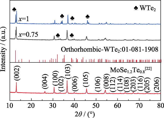
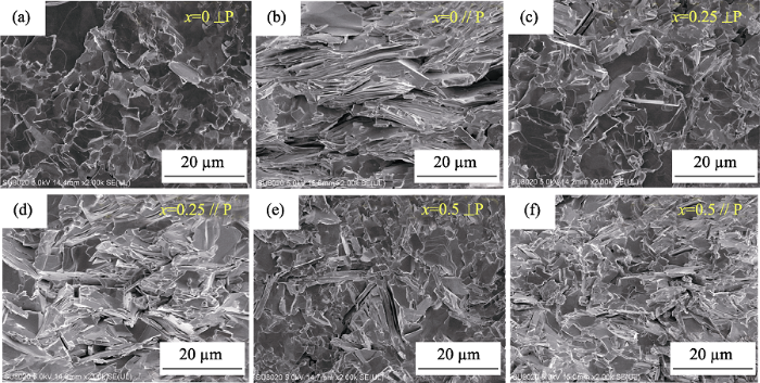
图1给出了Mo1-xWxSeTe固溶体(0≤x≤0.5)的粉末和块体XRD图谱。当0≤x≤0.5时, Mo1-xWxSeTe固溶体为六方结构, 没有明显的第二相, 与文献[22]报道的三元MoSeTe化合物晶型相同。而当x>0.5时, Mo1-xWxSeTe固溶体中析出了四方WTe2第二相, 见补充材料图S1。六方结构Mo1-xWxSeTe(0≤x≤0.5)固溶体具有层状结构, 层间为弱范德华作用力, 因而其烧结块体具有很强的各向异性。相比//P方向, ⊥p方向表现出明显的(00l)择优取向, 其块体XRD的(00l)谱峰很强。烧结后块体的断面SEM照片显示, 产物沿⊥p方向晶粒呈片状分布, 而沿//P方向可观察到明显的层状结构, 见补充材料图S2。通过计算, x=0、x=0.25和x=0.5三个样品沿(00l)晶面的取向因子LF, 我们发现三个组分的固溶体均具有明显的(00l)择优取向, 其在⊥p方向的LF因子分别为0.58、0.34和0.23, 计算方法见补充材料。随着W固溶量增加, LF因子明显降低, 这是W固溶增加了晶格无序度的缘故, 与三元MoSeTe中发现的规律一致[22]。
图1
图1
Mo1-xWxSeTe(0≤x≤0.5)固溶体的XRD图谱
Fig. 1
XRD patterns of the prepared Mo1-xWxSeTe (0≤x≤0.5) solid solutions
(a) Powder; (b) Bulk-⊥p; (c) Bulk-//P
图S1
图S1
Mo1-xWxSeTe(x=0.75和1)的粉末XRD图谱
Fig. S1
Powder XRD patterns of the prepared Mo1-xWxSeTe (x=0.75 and 1)
图S2
图S2
Mo1-xWxSeTe不同方向的断面SEM形貌
Fig. S2
SEM fractured surface morphologies of Mo1-xWxSeTe
(a) x = 0, ⊥P; (b) x = 0, //P; (c) x = 0.25, ⊥P; (d) x = 0.25, //P; (e) x = 0.5, ⊥P; (f) x = 0.5, //P
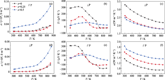
图2为Mo1-xWxSeTe(0≤x≤0.5)固溶体沿⊥p(a)和//P(b)方向的晶格热导率随温度变化的关系曲线。未掺杂的Mo1-xWxSeTe固溶体的s很低, 在整个温度范围内不超过1400 S·m-1(见补充材料图S3), 与三元MoSeTe固溶体类似[22]。根据Widmanm-Franz公式: κe=LsT(L为洛伦兹常数), 未掺杂的Mo1-xWxSeTe的κe很小。同时, 由于Mo1-xWxSeTe固溶体的Eg较大(~1.0 eV, 见补充材料表S1), 在测试温度范围内本征激发不显著, 导致κB也很小。因此, 未掺杂Mo1-xWxSeTe的κL近乎等于κ。结果表明, 所有Mo1-xWxSeTe固溶体的κL随着温度的升高而降低, 表明测试温度范围内声子的U散射主导样品的热传导过程。沿⊥p方向, Mo1-xWxSeTe固溶体的κL随W含量增加而显著降低, 而沿//P方向, 其κL随W含量增加而升高。一般而言, 对于强取向材料, 取向性越强, 则在两个方向的κL差值越大, 见图2所示。在择优方向κL相似时, 取向性更强的样品在非择优方向可取得更低的κL。因而, 高W含量样品在//P方向的κL相对较高, 是择优取向对非择优方向κL调节的结果。在Zhang等[22]的研究中, MoSe1.2Te0.8组分沿⊥p和//P两个方向的室温κL均达~2.78 W·m-1·K-1, 明显高于本研究中Mo0.5W0.5SeTe在⊥p和//P的~2.48和~1.83 W·m-1·K-1。这进一步证实, 在排除择优取向的影响后, W固溶本身依然会使Mo1-xWxSeTe固溶体的κL降低。
图2
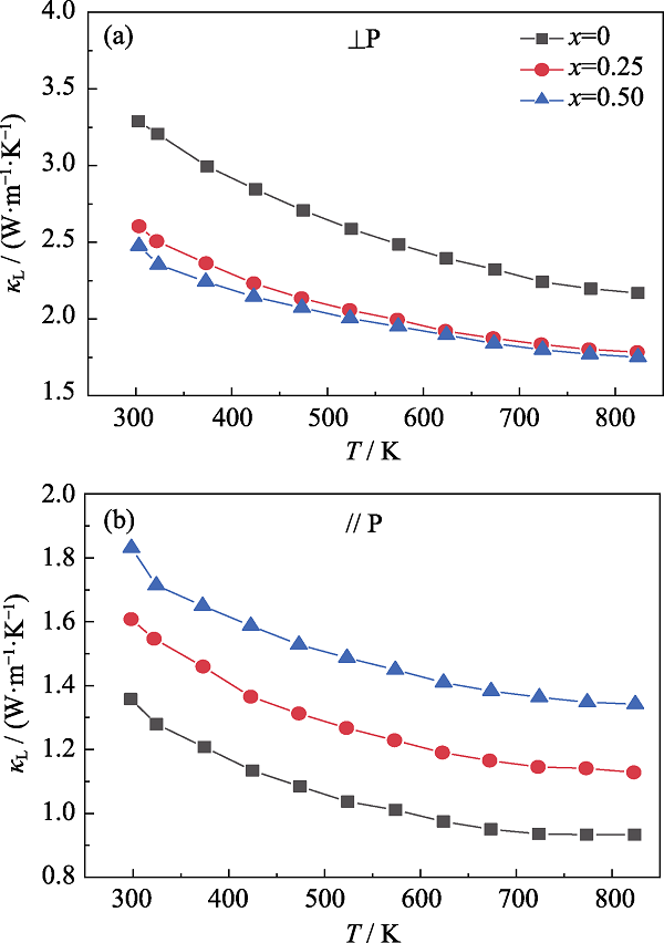
图2
Mo1-xWxSeTe(0≤x≤0.5)晶格热导率κL随温度T的变化曲线
Fig. 2
Temperature dependent lattice thermal conductivities of Mo1-xWxSeTe (0≤x≤0.5)
(a) ⊥p; (b) //P
图S3
图S3
Mo1-xWxSeTe 固溶体(0≤x≤0.5)沿⊥P和//P方向的(a, d)电导率σ, (b, e)塞贝克系数S和(c, f)热导率κ随温度变化的关系曲线
Fig. S3
Temperature dependence of (a, d) electrical conductivity σ, (b, e) Seebeck coefficient S, and (c, f) thermal conductivity κ of Mo1-xWxSeTe solid solutions (0≤x≤0.5) measured along the ⊥P and //P directions
图2为Mo1-xWxSeTe(0≤x≤0.5)固溶体沿⊥p(a)和//P(b)方向的晶格热导率随温度变化的关系曲线。未掺杂的Mo1-xWxSeTe固溶体的s很低, 在整个温度范围内不超过1400 S·m-1(见补充材料图S3), 与三元MoSeTe固溶体类似[22]。根据Widmanm-Franz公式: κe=LsT(L为洛伦兹常数), 未掺杂的Mo1-xWxSeTe的κe很小。同时, 由于Mo1-xWxSeTe固溶体的Eg较大(~1.0 eV, 见补充材料表S1), 在测试温度范围内本征激发不显著, 导致κB也很小。因此, 未掺杂Mo1-xWxSeTe的κL近乎等于κ。结果表明, 所有Mo1-xWxSeTe固溶体的κL随着温度的升高而降低, 表明测试温度范围内声子的U散射主导样品的热传导过程。沿⊥p方向, Mo1-xWxSeTe固溶体的κL随W含量增加而显著降低, 而沿//P方向, 其κL随W含量增加而升高。一般而言, 对于强取向材料, 取向性越强, 则在两个方向的κL差值越大, 见图2所示。在择优方向κL相似时, 取向性更强的样品在非择优方向可取得更低的κL。因而, 高W含量样品在//P方向的κL相对较高, 是择优取向对非择优方向κL调节的结果。在Zhang等[22]的研究中, MoSe1.2Te0.8组分沿⊥p和//P两个方向的室温κL均达~2.78 W·m-1·K-1, 明显高于本研究中Mo0.5W0.5SeTe在⊥p和//P的~2.48和~1.83 W·m-1·K-1。这进一步证实, 在排除择优取向的影响后, W固溶本身依然会使Mo1-xWxSeTe固溶体的κL降低。
表S1 1 Mo1-xWxSeTe(0≤x≤0.5)固溶体的组成、晶胞参数与光学带隙
Table S1
| Sample | Actual composition | Lattice parameters/nm | Eg/eV |
|---|---|---|---|
| x=0 | MoSe1.02Te1.04 | a=0.35, c=1.367 | 1.030 |
| x=0.25 | Mo0.74W0.25Se0.9Te0.96 | a=0.3512, c=1.375 | 1.005 |
| x=0.5 | Mo0.54W0.46Se0.93Te0.94 | a=0.3.5, c=1.371 | 0.998 |
表S2 2 Mo1-xWxSeTe(0≤x≤0.5)固溶体的取向因子LF
Table S2
| Sample | P0 | P⊥ | LF |
|---|---|---|---|
| x=0 | 0.31 | 0.71 | 0.58 |
| x=0.25 | 0.30 | 0.54 | 0.34 |
| x=0.5 | 0.29 | 0.45 | 0.23 |
表S3 3 Nb2yMo0.5-yW0.5-ySeTe(0≤y≤0.035)固溶体的组成与晶胞参数
Table S3
| Sample | Actual composition | Lattice parameters/nm |
|---|---|---|
| Mo0.5W0.5SeTe | Mo0.54W0.46Se0.93Te0.94 | a=0.350, c=1.371 |
| Nb0.01Mo0.495W0.495SeTe | Mo0.53W0.47Se0.99Te1.09 | a=0.351, c=1.371 |
| Nb0.03Mo0.485W0.485SeTe | Nb0.03Mo0.51W0.46Se0.93Te0.96 | a=0.351, c=1.370 |
| Nb0.05Mo0.475W0.475SeTe | Nb0.04Mo0.44W0.52Se0.97Te0.95 | a=0.352, c=1.371 |
| Nb0.07Mo0.465W0.465SeTe | Nb0.05Mo0.51W0.43Se0.90Te0.86 | a=0.352, c=1.371 |
2.2 Nb2yMo0.5-yW0.5-ySeTe的热电输运性能
根据2.1的研究, 选择具有较小(00l)择优取向以及较低κL的Mo0.5W0.5SeTe四元固溶体进行Nb掺杂优化电性能和热电优值ZT的研究。并且, 由于Mo0.5W0.5SeTe固溶体在⊥p方向具有(00l)择优取向且LF因子~0.23, 其Nb掺杂产物(Nb2yMo0.5-yW0.5-ySeTe)的电输运性能和热输运性能具有各向异性的特征。因此, 本研究中, 我们选取⊥p方向系统研究了Nb掺杂对热电输运性能的影响规律(//P方向热电输运数据见补充材料图S4), 并在此基础上选取性能最优的两个组分研究了取向对热电性能的影响规律。
图S4
图S4
Nb2yMo0.5-yW0.5-ySeTe(0≤y≤0.035)固溶体沿//P方向的(a)电导率σ, (b)塞贝克系数S, (c)功率因子PF, (d)热导率κ, (e)晶格热导率κL和(f)ZT值随温度变化的关系曲线
Fig. S4
Temperature dependence of (a) electrical conductivity σ, (b) Seebeck coefficient S, (c) power factor PF, (d) thermal conductivity κ, (e) lattice thermal conductivity κL and (f) the ZT values of Nb2yMo0.5-yW0.5-ySeTe (0≤y≤0.035) solid solutions measured along the //P direction
图3为Nb2yMo0.5-yW0.5-ySeTe(y=0、0.005、0.015、0.025和0.035)固溶体的粉末XRD图谱。结果表明, 不同Nb掺杂量的Nb2yMo0.5-yW0.5-ySeTe固溶体均为结晶度良好的单相, 没有发现明显的第二相结构。如表1所示, Nb2yMo0.5-yW0.5-ySeTe固溶体的实际Nb含量随y值增大而增加, 说明Nb进入了Mo/W晶格位置。y=0.005的样品由于Nb掺杂量太低, 电子探针的WDS成分分析没有检测到Nb。通过Highscore软件对Nb2yMo0.5-yW0.5-ySeTe固溶体的XRD图谱进行结构精修, 并计算晶胞参数(见补充材料表S3), Mo0.5W0.5SeTe四元固溶体中Nb掺杂对a参数和c参数的影响均不明显, 在MoSe1.2Te0.8三元固溶体中掺杂Nb后a参数没有明显变化而c参数明显降低[22]。Nb掺杂样品的Hall系数为正值, 主要载流子为空穴, 表现出明显的p型传导特性, 且随Nb含量y增加, 载流子浓度p显著提高。室温下(表1), y=0.035组分的载流子浓度高达7.63´1020 cm-3, 相比本征样品提升1~2个数量级, 这证实Nb是MoSe2基化合物的有效p型掺杂元素。
图3
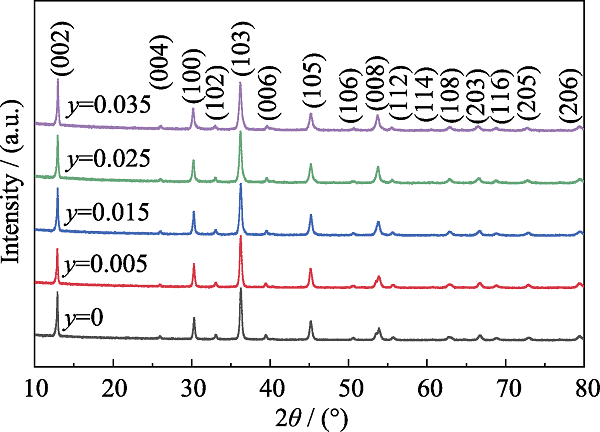
图3
Nb2yMo0.5-yW0.5-ySeTe(0≤y≤0.035)的粉末XRD图谱
Fig. 3
Powder XRD patterns of the prepared Nb2yMo0.5-yW0.5-ySeTe (0≤y≤0.035) solid solutions
表1 Nb2yMo0.5-yW0.5-ySeTe (0≤y≤0.035)固溶体的组成和室温热电输运性质
Table 1
| Sample | Actual composition | p/(×1020, cm-3) | μ/(cm2·V-1·s-1) | σ/(×104, S·m-1) | S/(μV·K-1) | |||
|---|---|---|---|---|---|---|---|---|
| ⊥P | //P | ⊥P | //P | ⊥P | //P | |||
| y=0 | Mo0.54W0.46Se0.93Te0.94 | 0.16 | 0.79 | 0.26 | 0.02 | 0.01 | 22.4 | 42.0 |
| y=0.005 | Mo0.53W0.47Se0.99Te1.09 | 1.53 | 1.37 | 1.32 | 0.33 | 0.32 | 17.2 | 15.1 |
| y=0.015 | Nb0.03Mo0.51W0.46Se0.93Te0.96 | 5.96 | 2.95 | 2.52 | 2.82 | 2.40 | 102 | 93.1 |
| y=0.025 | Nb0.04Mo0.44W0.52Se0.97Te0.95 | 6.61 | 5.45 | 4.80 | 5.76 | 5.07 | 65.9 | 70.9 |
| y=0.035 | Nb0.05Mo0.51W0.43Se0.90Te0.86 | 7.63 | 5.72 | 4.29 | 6.98 | 5.24 | 53.2 | 52.0 |
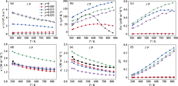
图4(a)为Nb2yMo0.5-yW0.5-ySeTe(y=0、0.005、0.015、0.025和0.035)固溶体沿⊥p方向的电导率随温度的变化关系曲线。结果表明(表1), 随Nb含量增加, Nb2yMo0.5-yW0.5-ySeTe固溶体的s提高了2~3个数量级, 室温下由本征样品的200 S·m-1提升至6.98×10⁴ S·m-1, 这主要是载流子浓度提高的缘故。由图4(a)可知, 当掺杂量y≤0.005时, Nb2yMo0.5-yW0.5-ySeTe固溶体的s随温度升高而增大, 表现为本征半导体传导特性; 而当y≥0.015时, 固溶体的s随温度升高而降低, 表现为重掺杂简并半导体传导特性。由表1可知, Nb掺杂不仅提高了载流子浓度p, 也显著提高了载流子迁移率μ, 这违背了载流子迁移率与载流子浓度变化趋势相反的一般规律。Zhang等[23]和Mott等[24]对V、Nb和Ta掺杂MoSe2的研究发现, V、Nb和Ta掺杂在浅掺杂情况下引入了离散的掺杂能级, 而在重掺杂情况下引入了连续的杂质能带, 如图4(a)中插图所示, 这引起p与μ随掺杂量增加而同步增大。Nb2yMo0.5-yW0.5-ySeTe固溶体中p与μ之间的反常变化关系也源于此。
图4
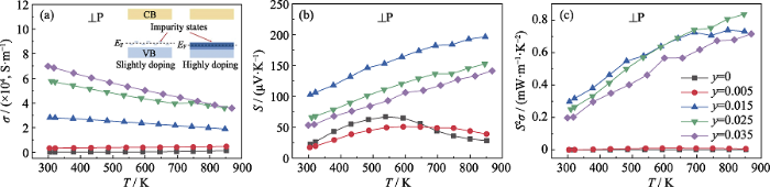
图4
Nb2yMo0.5-yW0.5-ySeTe(0≤y≤0.035)固溶体的(a)电导率s, (b)塞贝克系数S和(c)功率因子PF随温度的变化关系曲线, (a)中插图为Nb掺杂后引入的杂质能级示意图。
Fig. 4
Temperature dependence of (a) electrical conductivity s, (b) Seebeck coefficient S and (c) power factor PF of Nb2yMo0.5-yW0.5-ySeTe (0≤y≤0.035) solid solutions with inset in (a) showing the impurity states introduced by the Nb doping.
图4(b)为Nb2yMo0.5-yW0.5-ySeTe(y=0、0.005、0.015、0.025和0.035)固溶体沿⊥p方向的Seebeck系数随温度的变化关系。当掺杂量y≤0.005时, Nb2yMo0.5-yW0.5-ySeTe固溶体的S很小且随温度升高先增大后减小, 拐点出现在~600 K。这与低掺杂量条件下的离散掺杂能级有关: 离散杂质能级的电子态密度较小导致S较低, 且价带顶与离散杂质能级之间的载流子激发使得S在较低温度即出现拐点。当y≥0.015时, Nb2yMo0.5-yW0.5-ySeTe固溶体的S和传统简并半导体类似: 随掺杂量增加, 样品的S降低, 且样品的S随温度升高而增加。由图4(c)可知, Nb掺杂大幅提升了本征Mo0.5W0.5SeTe较低的s, 掺杂后Nb2yMo0.5-yW0.5-ySeTe的功率因子PF(PF=S2s)得到了明显的提升。除y=0.005的样品由于Nb含量过少, 未能达到良好的受主掺杂的效果外, 其余Nb掺杂量的PF都有显著提升。与S变化的规律类似, 掺杂后样品的PF随着温度的升高而增大, y=0.025的样品在823 K时获得最大PF, 达到0.84 mW·m-1·K-2, 与MoSeTe三元固溶体[22]相当, 明显高于MoSe2二元化合物[23]。
根据经典单抛物带模型可知, 简并半导体的Seebeck系数与载流子浓度以及载流子有效质量有关。图5为Nb2yMo0.5-yW0.5-ySeTe固溶体沿⊥p方向的室温Seebeck系数和载流子浓度的相互关系。基于单抛物带模型, 假设声学声子散射主导载流子输运[5], 计算Nb2yMo0.5-yW0.5-ySeTe固溶体的Pisarenko曲线, 如图5中实线所示。结果表明, Nb2yMo0.5-yW0.5-ySeTe固溶体的载流子有效质量较未掺杂样品有明显提升, 其值在2.2m0~3.5m0之间。并且, 高Nb掺杂量的Mo0.5W0.5SeTe四元固溶体的载流子有效质量较MoSeTe三元固溶体(m*=2.2m0~2.7m0)[22]和MoSe2二元化合物(m*=1.0m0~2.3 m0)[23]有所提高, 这有利于该四元固溶体获得更高的功率因子(PFµ(m*)2/3m)。Nb2yMo0.5-yW0.5-ySeTe四元掺杂固溶体中高的载流子有效质量可能是由于Nb掺杂引入的杂质能带具有更高的载流子有效质量。
图5
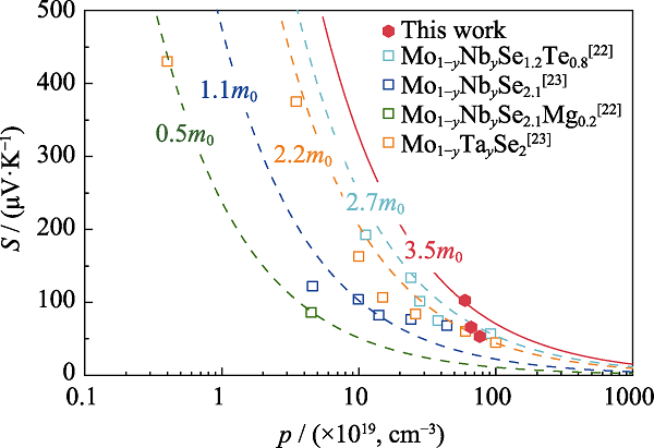
图5
Nb2yMo0.5-yW0.5-ySeTe(0≤y≤0.035)与文献报道的其它化合物的Pisarenko曲线对比
Fig. 5
Pisarenko plots for Nb2yMo0.5-yW0.5-ySeTe (0≤y≤0.035) samples compared with the reported data
图6为Nb2yMo0.5-yW0.5-ySeTe(y=0、0.005、0.015、0.025和0.035)固溶体沿⊥p方向的热导率(a)和晶格热导率(b)以及ZT(c)随温度的变化关系。结果表明, 随着Nb掺杂量的增加, Nb2yMo0.5-yW0.5-ySeTe固溶体的κ同时增大, 这主要是由于掺杂Nb后固溶体的s得到了大幅提升, κe随之增加的缘故。由于Mo0.5W0.5SeTe固溶体的Eg较大(0.998 eV, 见补充材料表S1), y≥0.015样品在测试温度区域内不会出现显著的本征激发, 这与S随温度升高也没有出现拐点的现象一致, 因而y≥0.015组分固溶体的κ不包含双极热导κB的贡献。同时, y≤0.005组分固溶体的κ随温度升高单调降低, 表明由于禁带宽度较大以及价带顶与杂质能级之间的载流子激发不显著, 其双极热导κB的贡献也不明显。因此, Nb2yMo0.5-yW0.5-ySeTe固溶体的κ主要来源于κe和κL的贡献。随温度升高, Nb2yMo0.5-yW0.5-ySeTe固溶体的κL单调降低, 近乎符合κLµT-1, 说明测量温度范围内κL由声子的U散射过程主导。结果也表明, 在一定掺杂浓度范围内, Nb掺杂引入的质量波动和应力场波动散射能适当降低样品的κL。例如, y=0.025的样品在室温和 823 K时的κL分别为2.3和1.65 W·m-1·K-1, 较本征Mo0.5W0.5SeTe的2.48和1.75 W·m-1·K-1都有一定程度的降低。
图6
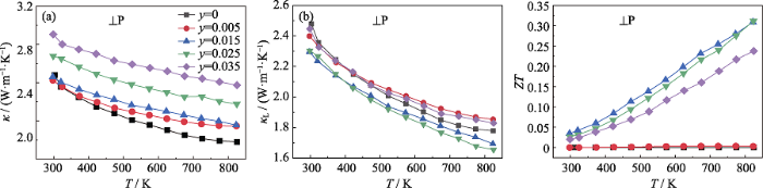
图6
Nb2yMo0.5-yW0.5-ySeTe(0≤y≤0.035)固溶体的(a)热导率κ, (b)晶格热导率κL和(c)ZT值随温度变化关系曲线
Fig. 6
Temperature dependent (a) thermal conductivity κ, (b) lattice thermal conductivity κL and (c) figure of merit ZT for Nb2yMo0.5-yW0.5-ySeTe (0≤y≤0.035) solid solutions
由于Nb掺杂能同步提高p与μ, Nb2yMo0.5-yW0.5-ySeTe固溶体的s和PF均获得了显著的提升; 再结合Nb掺杂能适当降低样品的κL, Nb2yMo0.5-yW0.5-ySeTe固溶体的ZT获得了明显优化。最终, y=0.015和y=0.025组分样品在823 K时取得最大ZT~0.31, 较未掺杂样品有了大幅度提升。
前文提及, Nb2yMo0.5-yW0.5-ySeTe固溶体的微结构具有明显的(00l)择优取向。因而, 我们对y=0.015和y=0.025两个性能优化的组分进行了不同方向上的热电输运性能比较(见补充材料图S5)。结果表明, Nb2yMo0.5-yW0.5-ySeTe固溶体在⊥p方向具有更高的s, 验证了此方向上的(00l)择优取向特征, 也说明了不同方向s的差别来源于载流子迁移率的差异(见表1)。同时, S没有表现明显的择优取向, 两个方向的S数值基本一致。此外, Nb2yMo0.5-yW0.5-ySeTe固溶体的κ和κL 具有明显取向性, ⊥p方向的数值更高, 这显然是(00l)择优取向的结果。归纳可知, 虽然Nb2yMo0.5-yW0.5-ySeTe固溶体在⊥p方向具有更高的s和PF, 但是的κ和κL也更高, 因此在//P方向的ZT反而相对略高。y=0.015的Nb0.03Mo0.485W0.485SeTe固溶体在823 K和//P方向获得最大ZT(0.36), 略优于⊥p方向ZT(0.31)。
图S5
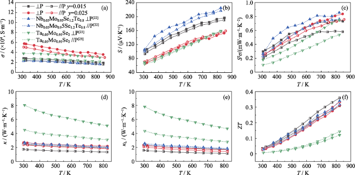
图S5
Nb2yMo0.5-yW0.5-ySeTe(y=0.015和0.025)固溶体和文献报道的Nb0.05Mo0.95SeTe和Ta0.05Mo0.95Se2沿⊥p和//P方向的热电性能比较
Fig. S5
Comparison of thermoelectric properties along ⊥p and //P directions among Nb2yMo0.5-yW0.5-ySeTe solid solutions with y=0.015 and 0.025 as well as Nb0.05Mo0.95SeTe and Ta0.05Mo0.95Se2 in the previous reports
(a) Electrical conductivity s; (b) Seebeck coefficient S; (c) Power factor PF; (d) Thermal conductivity κ; (e) Lattice thermal conductivity κL; (f) ZT
本研究中获得的Nb2yMo0.5-yW0.5-ySeTe固溶体的LF因子为~0.30, 明显低于文献报道三元MoSeTe的~0.40以及二元MoSe2的~0.70[22], 具有最低的(00l)择优取向。由于取向度和固溶的共同影响, 二元化合物Ta0.05Mo0.95Se2的κL明显高于三元固溶体和四元固溶体; 且Nb0.03Mo0.485W0.485SeTe在//P方向获得了所有产物中最低的κL。同等掺杂量条件下, 四元固溶体Nb0.05Mo0.475W0.475SeTe的p为6.61×1020 cm-3, 明显高于文献报道的三元固溶体(3.8×1020 cm-3)[22]和二元化合物(5.3×1020 cm-3)[23]的p。三元固溶体的p最低, S最高以及PF略高于四元组分, 而二元化合物的s和S均不突出, 导致其PF最低。本研究中Nb0.03Mo0.485W0.485SeTe和Nb0.05Mo0.475W0.475SeTe样品的PF都处于最高水平。并且, Nb0.03Mo0.485W0.485SeTe沿//P方向的κL最低, 因此其获得了所有产物中最高的热电优值, ZT达到0.36。
3 结论
本研究采用固相反应结合PAS烧结成功合成了一系列单相的Mo1-xWxSeTe(0≤x≤0.5)固溶体及其Nb掺杂产物, 探索了固溶结合掺杂对材料电输运和热输运性能的影响规律。结果发现, 在Mo位固溶W一方面明显降低了⊥p方向的(00l)择优取向, 另一方面也适当降低了Mo1-xWxSeTe固溶体的κL。在300和823 K时, W固溶量为0.5的Mo0.5W0.5SeTe固溶体在⊥p方向的κL分别为2.48和1.75 W·m-1·K-1, 较三元MoSeTe分别下降25%和18%。对Mo0.5W0.5SeTe固溶体的Nb掺杂研究表明, Nb掺杂显著提高了材料的s和PF, 适当地降低了κL, 进而显著提高了材料的热电优值ZT。Nb含量增加会同时提高p与μ, 这种反常变化趋势与Nb掺杂含量提高所引起的杂质能级由离散状态变成连续状态有关。此外, 取向性研究表明, Nb2yMo0.5-yW0.5-ySeTe固溶体在⊥p方向的s和PF更高, 但κ和κL也更高, 所以在//P方向反而获得相对更高的热电优值ZT。Nb0.03Mo0.485W0.485SeTe在823 K下⊥p和//P方向获得的最高ZT值分别达到0.31和0.36, 是目前MoSe2基热电材料中获得的最好结果之一。本研究证实, 固溶结合掺杂是优化MoSe2基材料热电性能的有效途径, 如能在优化的固溶组分下继续改善掺杂和提高PF, 将能进一步提升MoSe2基材料的ZT。
补充材料
本文相关补充材料可登陆https://doi.org/10.15541/ jim20200135查看。
取向因子LF的计算公式如下:
其中:
I(hkl)和I0(hkl)分别为测试样品块体及其粉末的全部谱峰的强度之和, 而I(00l)和I0(00l)则是(00l)晶面谱峰的强度之和。(00l)方向的峰强越高, 样品在(00l)方向的择优取向越明显。
不同于正文中提到的x≤0.5时产物为六方结构单相, 当x>0.5时, Mo1-xWxSeTe表现为六方结构和四方结构的混合物相。XRD图谱中标梅花符号处为WTe2四方相杂峰。在二元WTe2中, 由于强自旋轨道耦合的作用, 其六方相的三菱柱结构难以稳定存在, 因而二元WTe2的稳定结构为四方相结构。这也解释了高W含量的Mo1-xWxSeTe表现为混相结构的原因。
参考文献
Cooling, heating, generating power, and recovering waste heat with thermoelectric systems
DOI:10.1126/science.1158899
URL
PMID:18787160
[本文引用: 1]

Thermoelectric materials are solid-state energy converters whose combination of thermal, electrical, and semiconducting properties allows them to be used to convert waste heat into electricity or electrical power directly into cooling and heating. These materials can be competitive with fluid-based systems, such as two-phase air-conditioning compressors or heat pumps, or used in smaller-scale applications such as in automobile seats, night-vision systems, and electrical-enclosure cooling. More widespread use of thermoelectrics requires not only improving the intrinsic energy-conversion efficiency of the materials but also implementing recent advancements in system architecture. These principles are illustrated with several proven and potential applications of thermoelectrics.
Technologies and applications of thermoelectric devices: current status, challenges and prospects
DOI:10.15541/jim20180465
URL
[本文引用: 1]
Thermoelectric (TE) power generation technology is highly expected for various applications such as special power supply, green energy, energy harvesting from the environment and harvesting of industrial waste heat. Over the past years, the record of zT values of TE materials has been continuously updated, which would bode well for widespread practical applications of TE technology. However, the TE device as the core technology for the TE application lags behind the development of TE materials. Especially, the large-scale application of TE power generation technology is facing bottlenecks and new challenges. This reviewpresents an overview of the recent progress on TE device design and integration with particular attentions on device optimization design, electrode fabrication, interface engineering, and service behavior. The future challenges and development strategies for large-scale application ofthermoelectric power generation are also discussed.
Recent progress of thermoelectric nano-composites
Complex thermoelectric materials
DOI:10.1038/nmat2090
URL
PMID:18219332
[本文引用: 2]
Thermoelectric materials, which can generate electricity from waste heat or be used as solid-state Peltier coolers, could play an important role in a global sustainable energy solution. Such a development is contingent on identifying materials with higher thermoelectric efficiency than available at present, which is a challenge owing to the conflicting combination of material traits that are required. Nevertheless, because of modern synthesis and characterization techniques, particularly for nanoscale materials, a new era of complex thermoelectric materials is approaching. We review recent advances in the field, highlighting the strategies used to improve the thermopower and reduce the thermal conductivity.
High-performance bulk thermoelectrics with all-scale hierarchical architectures
DOI:10.1038/nature11439
URL
PMID:22996556
[本文引用: 1]
With about two-thirds of all used energy being lost as waste heat, there is a compelling need for high-performance thermoelectric materials that can directly and reversibly convert heat to electrical energy. However, the practical realization of thermoelectric materials is limited by their hitherto low figure of merit, ZT, which governs the Carnot efficiency according to the second law of thermodynamics. The recent successful strategy of nanostructuring to reduce thermal conductivity has achieved record-high ZT values in the range 1.5-1.8 at 750-900 kelvin, but still falls short of the generally desired threshold value of 2. Nanostructures in bulk thermoelectrics allow effective phonon scattering of a significant portion of the phonon spectrum, but phonons with long mean free paths remain largely unaffected. Here we show that heat-carrying phonons with long mean free paths can be scattered by controlling and fine-tuning the mesoscale architecture of nanostructured thermoelectric materials. Thus, by considering sources of scattering on all relevant length scales in a hierarchical fashion--from atomic-scale lattice disorder and nanoscale endotaxial precipitates to mesoscale grain boundaries--we achieve the maximum reduction in lattice thermal conductivity and a large enhancement in the thermoelectric performance of PbTe. By taking such a panoscopic approach to the scattering of heat-carrying phonons across integrated length scales, we go beyond nanostructuring and demonstrate a ZT value of approximately 2.2 at 915 kelvin in p-type PbTe endotaxially nanostructured with SrTe at a concentration of 4 mole per cent and mesostructured with powder processing and spark plasma sintering. This increase in ZT beyond the threshold of 2 highlights the role of, and need for, multiscale hierarchical architecture in controlling phonon scattering in bulk thermoelectrics, and offers a realistic prospect of the recovery of a significant portion of waste heat.
Rationally designing high-performance bulk thermoelectric materials
Multi-scale microstructural thermoelectric materials: transport behavior, non-equilibrium preparation, and applications
DOI:10.1002/adma.v29.20 URL [本文引用: 1]
High-thermoelectric performance of nanostructured bismuth antimony telluride bulk alloys
DOI:10.1126/science.1156446
URL
PMID:18356488
[本文引用: 2]
The dimensionless thermoelectric figure of merit (ZT) in bismuth antimony telluride (BiSbTe) bulk alloys has remained around 1 for more than 50 years. We show that a peak ZT of 1.4 at 100 degrees C can be achieved in a p-type nanocrystalline BiSbTe bulk alloy. These nanocrystalline bulk materials were made by hot pressing nanopowders that were ball-milled from crystalline ingots under inert conditions. Electrical transport measurements, coupled with microstructure studies and modeling, show that the ZT improvement is the result of low thermal conductivity caused by the increased phonon scattering by grain boundaries and defects. More importantly, ZT is about 1.2 at room temperature and 0.8 at 250 degrees C, which makes these materials useful for cooling and power generation. Cooling devices that use these materials have produced high-temperature differences of 86 degrees , 106 degrees , and 119 degrees C with hot-side temperatures set at 50 degrees, 100 degrees, and 150 degrees C, respectively. This discovery sets the stage for use of a new nanocomposite approach in developing high-performance low-cost bulk thermoelectric materials.
Convergence of electronic bands for high performance bulk thermoelectrics
DOI:10.1038/nature09996
URL
PMID:21544143
[本文引用: 2]
Thermoelectric generators, which directly convert heat into electricity, have long been relegated to use in space-based or other niche applications, but are now being actively considered for a variety of practical waste heat recovery systems-such as the conversion of car exhaust heat into electricity. Although these devices can be very reliable and compact, the thermoelectric materials themselves are relatively inefficient: to facilitate widespread application, it will be desirable to identify or develop materials that have an intensive thermoelectric materials figure of merit, zT, above 1.5 (ref. 1). Many different concepts have been used in the search for new materials with high thermoelectric efficiency, such as the use of nanostructuring to reduce phonon thermal conductivity, which has led to the investigation of a variety of complex material systems. In this vein, it is well known that a high valley degeneracy (typically
Grain boundary engineering with nano-scale InSb producing high performance InxCeyCo4Sb12+z skutterudite thermoelectrics
DOI:10.1016/j.jmat.2017.07.003 URL [本文引用: 2]
Convergence of conduction bands as a means of enhancing thermoelectric performance of n-type Mg2Si1-xSnx solid solutions
DOI:10.1103/PhysRevLett.108.166601
URL
PMID:22680741
[本文引用: 2]
Mg(2)Si and Mg(2)Sn are indirect band gap semiconductors with two low-lying conduction bands (the lower mass and higher mass bands) that have their respective band edges reversed in the two compounds. Consequently, for some composition x, Mg(2)Si(1-x)Sn(x) solid solutions must display a convergence in energy of the two conduction bands. Since Mg(2)Si(1-x)Sn(x) solid solutions are among the most prospective of the novel thermoelectric materials, we aim on exploring the influence of such a band convergence (valley degeneracy) on the Seebeck coefficient and thermoelectric properties in a series of Mg(2)Si(1-x)Sn(x) solid solutions uniformly doped with Sb. Transport measurements carried out from 4 to 800 K reveal a progressively increasing Seebeck coefficient that peaks at x=0.7. At this concentration the thermoelectric figure of merit ZT reaches exceptionally large values of 1.3 near 700 K. Our first principles calculations confirm that at the Sn content x approximately 0.7 the two conduction bands coincide in energy. We explain the high Seebeck coefficient and ZT values as originating from an enhanced density-of-states effective mass brought about by the increased valley degeneracy as the two conduction bands cross over. We corroborate the increase in the density-of-states effective mass by measurements of the low temperature specific heat. The research suggests that striving to achieve band degeneracy by means of compositional variations is an effective strategy for enhancing the thermoelectric properties of these materials.
High thermoelectric performance in low-cost SnS0.91Se0.09 crystals
DOI:10.1126/science.aax5123
URL
PMID:31604269
[本文引用: 2]
Thermoelectric technology allows conversion between heat and electricity. Many good thermoelectric materials contain rare or toxic elements, so developing low-cost and high-performance thermoelectric materials is warranted. Here, we report the temperature-dependent interplay of three separate electronic bands in hole-doped tin sulfide (SnS) crystals. This behavior leads to synergistic optimization between effective mass (m*) and carrier mobility (mu) and can be boosted through introducing selenium (Se). This enhanced the power factor from ~30 to ~53 microwatts per centimeter per square kelvin (muW cm(-1) K(-2) at 300 K), while lowering the thermal conductivity after Se alloying. As a result, we obtained a maximum figure of merit ZT (ZT max) of ~1.6 at 873 K and an average ZT (ZT ave) of ~1.25 at 300 to 873 K in SnS0.91Se0.09 crystals. Our strategy for band manipulation offers a different route for optimizing thermoelectric performance. The high-performance SnS crystals represent an important step toward low-cost, Earth-abundant, and environmentally friendly thermoelectrics.
Realizing high figure of merit in heavy-band p-type half-Heusler thermoelectric materials
Revelation of inherently high mobility enables Mg3Sb2 as a sustainable alternative to n-Bi2Te3 thermoelectrics
DOI:10.1002/advs.201802286
URL
PMID:31453051
[本文引用: 2]
Over the past years, thermoelectric Mg3Sb2 alloys particularly in n-type conduction, have attracted increasing attentions for thermoelectric applications, due to the multivalley conduction band, abundance of constituents, and less toxicity. However, the high vapor pressure, causticity of Mg, and the high melting point of Mg3Sb2 tend to cause the inclusion in the materials of boundary phases and defects that affect the transport properties. In this work, a utilization of tantalum-sealing for melting enables n-type Mg3Sb2 alloys to show a substantially higher mobility than ever reported, which can be attributed to the purification of phases and to the coarse grains. Importantly, the inherently high mobility successfully enables the thermoelectric figure of merit in optimal compositions to be highly competitive to that of commercially available n-type Bi2Te3 alloys and to be higher than that of other known n-type thermoelectrics at 300-500 K. This work reveals Mg3Sb2 alloys as a top candidate for near-room-temperature thermoelectric applications.
Electronics and optoelectronics of two-dimensional transition metal dichalcogenides
DOI:10.1038/NNANO.2012.193
URL
[本文引用: 1]
The remarkable properties of graphene have renewed interest in inorganic, two-dimensional materials with unique electronic and optical attributes. Transition metal dichalcogenides (TMDCs) are layered materials with strong in-plane bonding and weak out-of-plane interactions enabling exfoliation into two-dimensional layers of single unit cell thickness. Although TMDCs have been studied for decades, recent advances in nanoscale materials characterization and device fabrication have opened up new opportunities for two-dimensional layers of thin TMDCs in nanoelectronics and optoelectronics. TMDCs such as MoS2, MoSe2, WS2 and WSe2 have sizable bandgaps that change from indirect to direct in single layers, allowing applications such as transistors, photodetectors and electroluminescent devices. We review the historical development of TMDCs, methods for preparing atomically thin layers, their electronic and optical properties, and prospects for future advances in electronics and optoelectronics.
Electronic and thermoelectric properties of few-layer transition metal dichalcogenides
DOI:10.1063/1.4869142
URL
PMID:24697473
[本文引用: 1]
The electronic and thermoelectric properties of one to four monolayers of MoS2, MoSe2, WS2, and WSe2 are calculated. For few layer thicknesses, the near degeneracies of the conduction band K and Sigma valleys and the valence band Gamma and K valleys enhance the n-type and p-type thermoelectric performance. The interlayer hybridization and energy level splitting determine how the number of modes within kBT of a valley minimum changes with layer thickness. In all cases, the maximum ZT coincides with the greatest near-degeneracy within kBT of the band edge that results in the sharpest turn-on of the density of modes. The thickness at which this maximum occurs is, in general, not a monolayer. The transition from few layers to bulk is discussed. Effective masses, energy gaps, power-factors, and ZT values are tabulated for all materials and layer thicknesses.
Enhancement of anisotropic thermoelectric performance of tungsten disulfide by titanium doping
DOI:10.1039/C6TA03122F URL [本文引用: 1]
Dramatically enhanced thermoelectric performance of MoS2 by introducing MoO2 nanoinclusions
DOI:10.1039/C6TA10219K URL [本文引用: 1]
Realizing p-type MoS2 with enhanced thermoelectric performance by embedding VMo2S4 nanoinclusions
DOI:10.1021/acs.jpcb.7b06379
URL
PMID:28825829
[本文引用: 1]
Two-dimensional transition-metal dichalcogenide semiconductors (TMDCs) such as MoS2 are attracting increasing interest as thermoelectric materials owing to their abundance, nontoxicity, and promising performance. Recently, we have successfully developed n-type MoS2 thermoelectric material via oxygen doping. Nevertheless, an efficient thermoelectric module requires both n-type and p-type materials with similar compatibility factors. Here, we present a facile approach to obtain a p-type MoS2 thermoelectric material with a maximum figure of merit of 0.18 through the introduction of VMo2S4 as a second phase by vanadium doping. VMo2S4 nanoinclusions, confirmed by X-ray powder diffraction (XRD) and transmission electron microscopy (TEM) measurements, not only improve the electrical conductivity by simultaneously increasing the carrier concentration and the mobility but also result in the reduction of lattice thermal conductivity by enhancing the interface phonon scattering. Our studies not only shed new light toward improving thermoelectric performance of TMDCs by a facile elemental doping strategy but also pave the way toward thermoelectric devices based on TMDCs.
Enhancement of thermoelectric properties of molybdenum diselenide through combined Mg intercalation and Nb doping
DOI:10.1007/s11664-016-4334-7 URL [本文引用: 1]
Synergistically improved electronic and thermal transport properties in Nb-doped NbyMo1-ySe2-2xTe2x solid solutions due to alloy phonon scattering and increased valley degeneracy
DOI:10.1021/acsami.9b03681
URL
PMID:31242387
[本文引用: 12]
The layered 2H-MoSe2-based compounds have recently attracted considerable attention as novel thermoelectric (TE) materials for medium-to-high temperature power generation. In this research, for the first time, dissolving Te in binary MoSe2 and thus forming MoSe2-2xTe2x solid solutions is shown to be very effective for reducing lattice thermal conductivity (kappaL) due to strong alloy scattering of phonons. Along the perpendicularP direction, MoSe1.2Te0.8 achieves the lowest kappaL of 2.87 W m(-1) K(-1) at room temperature among all solid solutions, an 85% decrease from that of pristine MoSe2 (18.69 W m(-1) K(-1)). Band structure calculations and experiments have verified that Te alloying effectively increases the density-of-states effective mass of MoSe2-2xTe2x solid solutions via increased valley degeneracy, leading to an enhanced Seebeck coefficient. Moreover, Nb doping modulates the density of holes of NbyMo1-ySe1.2Te0.8 samples to its optimum level and gives rise to the maximum power factor of 0.85 mW m(-1) K(-2) at 823 K. On account of synergistic optimization of the electronic and thermal transport, Nb0.05Mo0.95Se1.2Te0.8 has achieved the highest ZT value of 0.34 at 823 K, representing a 70% enhancement as compared to the best result previously reported for MoSe2. This research documents that alloying combined with doping is an effective avenue to greatly enhance the TE performance of NbyMo1-ySe2-2xTe2x solid solutions.
Impurity states in Mo1-xMxSe2 compounds doped with group VB elements and their electronic and thermal transport properties
DOI:10.1039/C9TC05008F URL [本文引用: 5]
Electronic processes in non- crystalline materials
