

In 2004, Geim and Novoselov[1] successfully obtained the single-layer graphene material by mechanical exfoliation. It is first confirmed that the two-dimensional carbon material can exist alone. Graphene is an ideal two-dimensional material composed of a single-layer of carbon atoms, and its atoms form a six-carbon ring planar structure by sp2 hybridization[2]. Graphene is the basic unit of other carbon materials, and it can be wrapped up into fullerenes, rolled into carbon nanotubes or stacked into graphite. The thickness of a single-layer graphene is about 0.335 nm, which gives it excellent optical properties, electrical properties and mechanical properties[3,4,5]. For example, the single-layer graphene only absorbs 2.3% of the visible light, and it looks almost transparent. The carrier mobility of single-layer graphene at room temperature is about 15000 cm2/(V·s), which is 10 times higher than that of silicon. In addition, its Young’s modulus is up to 1 Tpa, and the compressive strength reaches 180 GPa, which is 100 times of ordinary steel. At the same time, the unique two-dimensional structure endows the graphene with excellent thermal properties[6,7,8]. The thermal conductivity of graphene theoretically reaches 5300 W/(m·K)[9], which is about 5 times of diamond, 10 times of copper, and 100 times of silicon. However, the excellent properties are closely related to the number of graphene layers. As the number of graphene layers increases, the performances of graphene, like absorption, carrier mobility, and Young’s modulus, are greatly reduced. For instance, the thermal conductivity of the graphene with ten layers is reduced to below 1000 W/(m·K)[10].
Up to now, there have been a variety of methods for preparing the graphene materials, mainly including the mechanical exfoliation[1], redox method[11,12], liquid phase exfoliation[13,14], epitaxial growth[15], chemical vapor deposition (CVD)[16,17,18] and so on. The mechanical exfoliation and liquid phase exfoliation methods have problems of low yield and high energy cost, while the size and morphology of graphene prepared by redox method are difficult to control and the quality is not guaranteed. The process of epitaxial growth of graphene is cumbersome. Compared with the mentioned methods above, CVD is the most effective method for obtaining high quality, large-sized graphene, which has the advantages of low cost and high yield[19,20]. By controlling the decomposition and deposition of carbon atoms at high temperature and low pressure, the structure and number of layers of graphene on catalyst substrate surface can be effectively controlled. Since the catalyst substrate provide the sites for graphene nucleation and growth, the surface features of the catalyst substrate, such as roughness[21], defects[22,23], grain size[24,25] and crystal plane orientation[26]etc., directly affect the quality and size of the final graphene.
The substrate pretreatment can significantly reduce the catalyst surface defects and impurities [27,28,29,30]. In this work, the effects of different Cu substrate pretreatment methods on the quality of graphene were studied, and the common pickling, passivation pickling paste and electrochemical polishing were compared. A novel method for treating copper substrates by the combination of passivation paste pickling and electrochemical polishing is proposed. The effects of working voltage and time on the Cu substrate in electrochemical polishing process were discussed. Then the effect of annealing process on the grain of Cu substrate was systematically studied. In addition, the structure morphologies of produced graphene films were characterized.
1 Experimental
1.1 Materials
The isopropyl alcohol, anhydrous ethanol, concentrated sulfuric acid, phosphoric acid and hydrochloric acid were purchased from Sinopharm Chemical Reagent Co., Ltd. (China). The polyethylene glycol, and glycerol were purchased from Shanghai Titan Chemical Co., Ltd. (China). The tributyl phosphate was purchased from Aladdin reagent Co., Ltd. (China), and the copper foil (purity 99.9%, thickness 100 μm) was from Chinalco Luoyang Copper Industry Co., Ltd. (China).
1.2 Pretreatment of copper substrates
In this work, different methods are used to pretreat copper substrate. The untreated copper foil was respectively washed in isopropyl alcohol, absolute ethanol, and deionized water via an ultrasonic for about 10 min. Then, 1) Etching treatment with hydrochloric acid. The sonicated copper foil was placed in 10% hydrochloric acid solution for 2 min, then rinsed with deionized water, and blown dry with nitrogen. 2) Hydrochloric acid etching and electrochemical polishing. Some copper foils etched by hydrochloric acid were furtherly electrochemically polished. The electropolishing time was set to 8 min and voltage to 8 V. The polishing liquid consisted of 100 g of phosphoric acid, 30 g of sulfuric acid, 5 g of hydrochloric acid, 8 g of polyethylene glycol, 5 g of glycerin, 25 g of deionized water, and 1 g of tributyl phosphate. 3) Etching treatment with passivation paste. The surface of copper foil was carefully scrubbed with the passivation paste, and the scrubbing time was set to 2 min. 4) Passivation paste etching and electrochemical polishing. A portion of copper foils treated with the passivation paste were subjected to electrochemical polishing treatment.
1.3 Graphene growth by CVD
The pretreated copper foil was placed in a horizontal quartz tube furnace (inner diameter of 100 mm). The system was evacuated to about 1.33 Pa, and then filled with 200 sccm of argon to atmospheric pressure. Argon (Ar, 99.999% purity) and 100 sccm hydrogen (H2, 99.999% purity) gas mixture was introduced for 10 min, then the temperature program started. When the temperature and pressure reach the desired values, methane was introduced (from 0.5 sccm to 5.0 sccm). The growth temperature was set to 1060 ℃, and the process was carried out for 25 min. Then, it was cooled to room temperature under an atmosphere of argon and hydrogen.
1.4 Characterization
The surface morphology of copper substrates and graphene samples were examined by an optical microscope (OM, DM2500M, Leica Instruments Co., Ltd.) and a scanning electron microscope (SEM, Hitach S-4800, Bruker). The graphene structure was tested by Raman spectroscopy ( XploRA PLUS, HORIBA, Japan).
2 Results and discussion
2.1 Different pretreatment on copper substrate
The copper substrates were treated by different methods, and the optical microscope images of different samples are shown in Fig. 1. As can be seen from Fig. 1(a), there are a large number of streaks and impurity defects on the surface of the untreated copper foil. From Fig. 1(b), the surface morphology of the copper foil does not change much, and the surface still has streaks and defects after etching with hydrochloric acid for 20 h. Therefore, the dilute hydrochloric acid etching treatment does not give the copper foil a smooth surface. When the copper foil is further processed by electrochemical polishing, the surface morphology of copper foil is changed significantly in Fig. 1(c). The original stripe disappears and the surface is more smooth. Fig. 1(d) is the photomicrograph of the copper foil treated with passivation paste. It can be seen that the corrosion effect is obvious and the surface morphology is completely changed, but the surface exhibits loose and rough appearance. Then the copper foil treated by the passivation paste is furtherly subjected to electrochemical polishing treatment. Surprisingly, the flatness and smoothness of the copper foil substrate are significantly improved, and the mirror effect is macroscopically achieved as shown in Fig. 1(e). So the combination of the passivation paste pickling and electrochemical polishing is an effective method for treating copper substrates.
Fig. 1
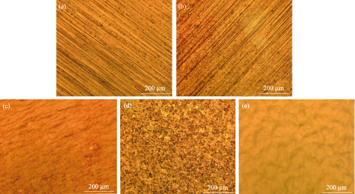
Fig. 1
OM images of different copper substrates
(a) Untreated copper substrate; (b) Hydrochloric acid etching treatment; (c) Hydrochloric acid etching and electrochemical polishing treatment; (d) Passivation paste etching; (e) Passivation paste etching and electrochemical polishing treatment
2.2 Effect of electrochemical polishing voltage and polishing time
In order to explore the process parameters of electrochemical polishing, the effect of polishing voltage and polishing time were studied. As shown in Fig. 2, three polishing voltages, 1.2, 4.0 and 8.0 V, were selected. It can be seen from Fig. 2(a1-a4) that when the polishing voltage is set to 1.2 V, electrochemical polishing treatment has little effect on the copper foil. There are still some defects such as streaks and pits on the surface of copper foils even if the polishing time increases to 40 min. When voltage is 4 V, the surface of the copper foil treated for 10 min changes significantly in Fig. 2(b1), and the streaks become shallow. With the polishing time increasing to 30 min, the streaks and defects on copper surface are completely removed as shown in Fig. 2(b3). However, the excessive corrosion pits appear if polishing time is up to 40 min. In Fig. 2(b4), it can be demonstrated that there are some corrosion pits on the surface of the copper foil. As the polishing voltage increasing to 8 V, the polishing time also has great influence on copper surface morphology. When the polishing time is 8 min, the surface of the copper foil substrate is flat and smooth as shown in Fig. 2(c1). The surface smoothness is improved significantly with the polishing time increasing, but excessive prolonging polishing time easily causes corrosion (Fig. 2(c2-c4)).
Fig. 2
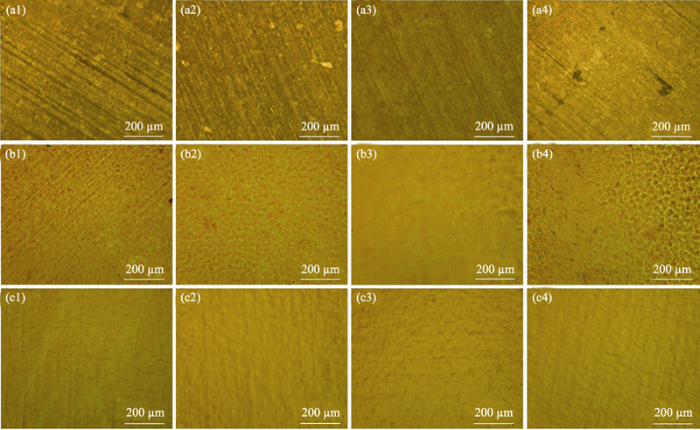
Fig. 2
OM images of copper substrates electrochemical polished with different voltages and time
(a1) 1.2 V/10 min; (a2) 1.2 V/20 min; (a3) 1.2 V/30 min; (a4) 1.2 V/40 min; (b1) 4 V/10 min; (b2) 4 V/20 min; (b3) 4 V/30 min; (b4) 4 V/40 min; (c1) 8 V/6 min; (c2) 8 V/8 min; (c3) 8 V/10 min; (c4) 8 V/12 min
Therefore, the copper foil cannot be significantly polished when the polishing voltage is too low, while the excessive polishing time causes excessive polishing with high voltage. Based on the results, the appropriate polishing voltage and time are set as 8 V and 8 min, respectively.
2.3 Effect of annealing temperature
In the growing process of graphene, the grain size and uniformity of copper catalyst have great influence on graphene quality and size. The temperature is a very important factor, and the annealing treatment can signifycantly improve the surface morphology of the copper foil substrate. The copper foils were annealed at different temperatures for 30 min. It can be seen from Fig. 3(a) that when the annealing is performed at 800 ℃ for 30 min, the grain is less than 100 μm in size and ununiform. As the annealing temperature rises to 900 ℃, the surface morphology of the copper foil substrate is slightly changed, and some grain become larger (~200 μm). But the annealing effect is still poor, and grain size is still uneven. When the annealing temperature is increased to 1000 and 1060 ℃, the grain size of the copper foil is larger and the uniformity is significantly improved, as shown in Fig. 3(c, d).
Fig. 3
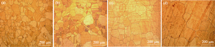
Fig. 3
OM images of copper substrates annealed at different temperatures for 30 min (a) 800 ℃; (b) 900 ℃; (c) 1000 ℃; (d) 1060 ℃
2.4 Effect of annealing time
In addition to annealing temperature, the annealing time also seriously affects copper grain size and its uniformity. When the annealing temperature is 1000 ℃ with no holding time, the grain is unevenly distributed with dimension less than 200 μm, as shown in Fig. 4(a). However, the grain becomes significantly larger as the annealing time is kept at 30 min, and most of the grains exceed 200 μm with improved uniformity (Fig. 4(b)). With the annealing time increasing to 90 or 120 min, Cu grains continue to increase (>400 μm), while the number of grains decreases (Fig. 4(c, d)). However, too long annealing time can increase energy cost. Considering the results from Fig. 3 and Fig. 4, the copper foil substrate with larger grain size and uniform distribution can be obtained by annealing at 1000 ℃ for 30 min.
Fig. 4
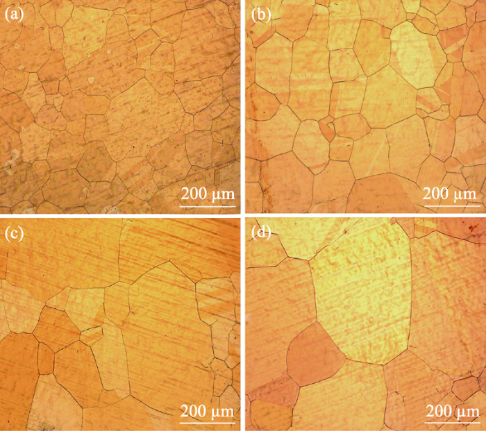
Fig. 4
OM images of copper substrates annealed at 1000 ℃ for different time (a) 0; (b) 30 min; (c) 90 min; (d) 120 min
2.5 Graphene characterization
SEM image of graphene sample by CVD growth is shown in Fig. 5. Two regions, gray and dark gray area are clearly visible, indicating that different layers of graphene are grown. In order to analyze the quality of the prepared graphene, the graphene in different regions are characterized by the Raman spectra (Fig. 6). The D peak in Raman spectra represents the defect peak of graphene, while the G peak represents the characteristic peak of carbon sp2, reflecting the crystallinity and symmetry. 2D is the second-order Raman scattering peak of the region boundary phonon, which is used to determine the existence of graphene. So the IG/ID demonstrates the degree of defect of the graphene crystal, and I2D/IG represents graphene layer. Fig. 6(a) is the Raman spectrum of the quartz substrate. The quartz substrate can produce a light scattering effect to cause characteristic peaks other than graphene in Fig. 6(b, c). Compared with the Raman spectrum of the graphene sample in gray area, the D band intensity of graphene in dark gray area is lower, while the 2D band intensity is significantly higher, as show in Fig. 6(b, c). In addition, the ID /IG is slightly decreased, and the I2D/IG is obviously increased in Table 1. Therefore, the graphene in dark gray area has fewer defects and better quality.
Fig. 5
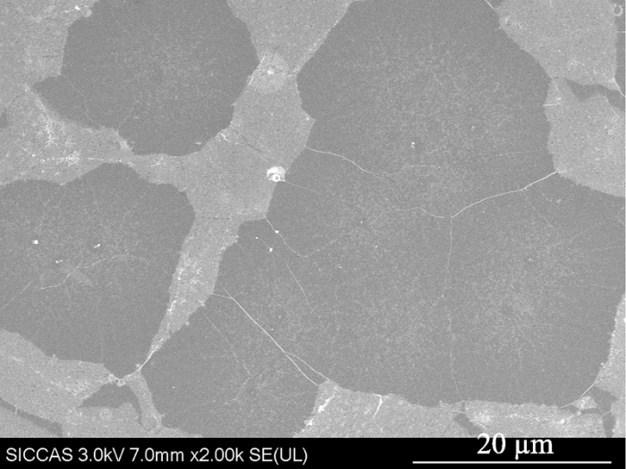
Fig. 6
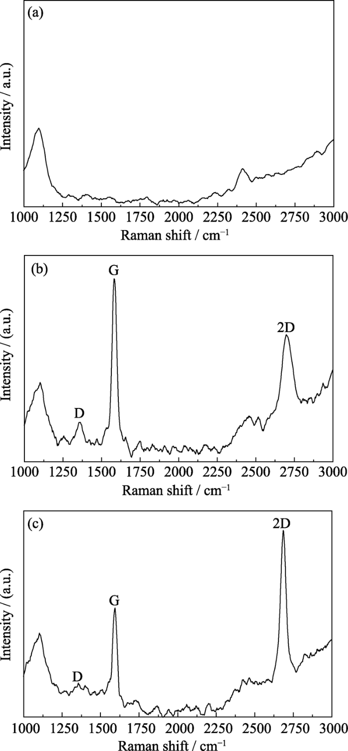
Fig. 6
Raman spectra of quartz substrate (a), graphene sample in gray area (b), and graphene sample in dark gray area (c)
3 Conclusion
The effects of different pretreatment on the surface morphology of copper substrates were studied. It can be found that the combined treatment of passivation paste pickling and electrochemical polishing can effectively remove surface defects on copper substrates. The influence of polishing process and annealing process parameters on the copper substrate are systematically demonstrated, and a process for preparing high-quality graphene by CVD is developed. According to the SEM image and Raman spectrum, the graphene film prepared in this work is few-layer, large-size, high-quality. It is worth emphasizing that the copper foil used in this work is the common copper foil, and its purity is only 99.9%. Overall, our work provides a novel method for large-scale preparation of high-quality graphene.
Table 1 Comparison of the Raman characteristic peak in different graphene areas
| Area | D band/cm-1 | G band/cm-1 | 2D band/cm-1 | ID/IG | I2D/IG |
|---|---|---|---|---|---|
| Gray area | 1354 | 1581 | 2697 | 0.57 | 0.83 |
| Dark gray area | 1354 | 1592 | 2684 | 0.26 | 1.29 |
参考文献
Electric field effect in atomically thin carbon films

We describe monocrystalline graphitic films, which are a few atoms thick but are nonetheless stable under ambient conditions, metallic, and of remarkably high quality. The films are found to be a two-dimensional semimetal with a tiny overlap between valence and conductance bands, and they exhibit a strong ambipolar electric field effect such that electrons and holes in concentrations up to 10(13) per square centimeter and with room-temperature mobilities of approximately 10,000 square centimeters per volt-second can be induced by applying gate voltage.
Direct growth of ultrafast transparent single-layer graphene defoggers
The idea flat surface, superb thermal conductivity and excellent optical transmittance of single-layer graphene promise tremendous potential for graphene as a material for transparent defoggers. However, the resistance of defoggers made from conventional transferred graphene increases sharply once both sides of the film are covered by water molecules which, in turn, leads to a temperature drop that is inefficient for fog removal. Here, the direct growth of large-area and continuous graphene films on quartz is reported, and the first practical single-layer graphene defogger is fabricated. The advantages of this single-layer graphene defogger lie in its ultrafast defogging time for relatively low input voltages and excellent defogging robustness. It can completely remove fog within 6 s when supplied a safe voltage of 32 V. No visible changes in the full defogging time after 50 defogging cycles are observed. This outstanding performance is attributed to the strong interaction forces between the graphene films and the substrates, which prevents the permeation of water molecules. These directly grown transparent graphene defoggers are expected to have excellent prospects in various applications such as anti-fog glasses, auto window and mirror defogging.
Optical characterization of directly deposited graphene on a dielectric substrate
By using scanning multiphoton microscopy we compare the nonlinear optical properties of the directly deposited and transferred to the dielectric substrate graphene. The direct deposition of graphene on oxidized silicon wafer was done by utilizing sacrificial copper catalyst film. We demonstrate that the directly deposited graphene and bi-layered transferred graphene produce comparable third harmonic signals and have almost the same damage thresholds. Therefore, we believe directly deposited graphene is suitable for the use of e.g. nanofabricated optical setups.
Large-area synthesis of high-quality and uniform graphene films on copper foils
Graphene has been attracting great interest because of its distinctive band structure and physical properties. Today, graphene is limited to small sizes because it is produced mostly by exfoliating graphite. We grew large-area graphene films of the order of centimeters on copper substrates by chemical vapor deposition using methane. The films are predominantly single-layer graphene, with a small percentage (less than 5%) of the area having few layers, and are continuous across copper surface steps and grain boundaries. The low solubility of carbon in copper appears to help make this growth process self-limiting. We also developed graphene film transfer processes to arbitrary substrates, and dual-gated field-effect transistors fabricated on silicon/silicon dioxide substrates showed electron mobilities as high as 4050 square centimeters per volt per second at room temperature.
Computer simulation of the thermal stability of nickel films on two-layer graphene
3D graphene fibers grown by thermal chemical vapor deposition
Enhanced thermoelectric conversion efficiency of cvd graphene with reduced grain sizes
Thermal transport in supported graphene nanomesh
Graphene is considered as a promising candidate material to replace silicon for the next-generation nanoelectronics because of its superb carrier mobility. To evaluate its thermal dissipation capability as electronic materials, the thermal transport in monolayer graphene was extensively explored over the past decade. However, the supported chemical vapor deposition (CVD) grown monolayer graphene with submicron structures were seldom studied, which is important for practical nanoelectronics. Here we investigate the thermal transport properties in a series of CVD graphene nanomeshes patterned by a hard-template-assisted etching method. The experimental and numerical results uncovered the phonon backscattering at hole boundary (<100 nm neck width) and its substantial contribution to the thermal conductivity reduction.
Superior thermal conductivity of single-layer graphene
We report the measurement of the thermal conductivity of a suspended single-layer graphene. The room temperature values of the thermal conductivity in the range approximately (4.84+/-0.44)x10(3) to (5.30+/-0.48)x10(3) W/mK were extracted for a single-layer graphene from the dependence of the Raman G peak frequency on the excitation laser power and independently measured G peak temperature coefficient. The extremely high value of the thermal conductivity suggests that graphene can outperform carbon nanotubes in heat conduction. The superb thermal conduction property of graphene is beneficial for the proposed electronic applications and establishes graphene as an excellent material for thermal management.
Large area, few-layer graphene films on arbitrary substrates by chemical vapor deposition
In this work we present a low cost and scalable technique, via ambient pressure chemical vapor deposition (CVD) on polycrystalline Ni films, to fabricate large area ( approximately cm2) films of single- to few-layer graphene and to transfer the films to nonspecific substrates. These films consist of regions of 1 to approximately 12 graphene layers. Single- or bilayer regions can be up to 20 mum in lateral size. The films are continuous over the entire area and can be patterned lithographically or by prepatterning the underlying Ni film. The transparency, conductivity, and ambipolar transfer characteristics of the films suggest their potential as another materials candidate for electronics and opto-electronic applications.
Preparation and characterization of polyamide-6/reduced graphene oxide composite microspheres
Preparation and characterization of platinum alloy catalysts supported on n-doped reduced graphene oxide for anode in direct ethanol fuel cell (DEFC)
The liquid-phase preparation of graphene by shear exfoliation with graphite oxide as a dispersant
Preparation, characterization, and application of electrochemically functional graphene nanocomposites by one-step liquid-phase exfoliation of natural flake graphite with methylene blue
Smooth epitaxial copper film on sapphire surface suitable for high quality graphene growth
A review of chemical vapour deposition of graphene on copper
Growth of graphene on Cu foils by microwave plasma chemical vapor deposition: the effect of in-situ hydrogen plasma post-treatment
Growth of single-layer graphene on Ge (100) by chemical vapor deposition
Controllable synthesis of submillimeter single-crystal monolayer graphene domains on copper foils by suppressing nucleation
Comparative analysis of graphene grown on copper and nickel sheet by microwave plasma chemical vapor deposition
Thermal properties of graphene- copper-graphene heterogeneous films
We demonstrated experimentally that graphene-Cu-graphene heterogeneous films reveal strongly enhanced thermal conductivity as compared to the reference Cu and annealed Cu films. Chemical vapor deposition of a single atomic plane of graphene on both sides of 9 mum thick Cu films increases their thermal conductivity by up to 24% near room temperature. Interestingly, the observed improvement of thermal properties of graphene-Cu-graphene heterofilms results primarily from the changes in Cu morphology during graphene deposition rather than from graphene's action as an additional heat conducting channel. Enhancement of thermal properties of graphene-capped Cu films is important for thermal management of advanced electronic chips and proposed applications of graphene in the hybrid graphene-Cu interconnect hierarchies.
Heat transport in low-dimensional materials: a review and perspective
Computation of the thermal resistance in graphene sheets with a rectangular hole
In-plane thermal conductivity of polycrystalline chemical vapor deposition graphene with controlled grain sizes
Manipulation of the chemical vapor deposition graphene synthesis conditions, such as operating P, T, heating/cooling time intervals, and precursor gas concentration ratios (CH4/H2), allowed for synthesis of polycrystalline single-layered graphene with controlled grain sizes. The graphene samples were then suspended on 8 mum diameter patterned holes on a silicon-nitride (Si3N4) substrate, and the in-plane thermal conductivities k(T) for 320 K < T < 510 K were measured to be 2660-1230, 1890-1020, and 680-340 W/m.K for average grain sizes of 4.1, 2.2, and 0.5 mum, respectively, using an opto-thermal Raman technique. Fitting of these data by a simple linear chain model of polycrystalline thermal transport determined k = 5500-1980 W/m.K for single-crystal graphene for the same temperature range above; thus, significant reduction of k was achieved when the grain size was decreased from infinite down to 0.5 mum. Furthermore, detailed elaborations were performed to assess the measurement reliability of k by addressing the hole-edge boundary condition, and the air-convection/radiation losses from the graphene surface.
Engineering polycrystalline Ni films to improve thickness uniformity of the chemical- vapor-deposition-grown graphene films
It has been shown that few-layer graphene films can be grown by atmospheric chemical vapor deposition using deposited Ni thin films on SiO(2)/Si substrates. In this paper we report the correlation between the thickness variations of the graphene film with the grain size of the Ni film. Further investigations were carried out to increase the grain size of a polycrystalline nickel film. It was found that the minimization of the internal stress not only promotes the growth of the grains with (111) orientation in the Ni film, but it also increases their grain size. Different types of SiO(2) substrates also affect the grain size development. Based upon these observations, an annealing method was used to promote large grain growth while maintaining the continuity of the nickel film. Graphene films grown from Ni films with large versus small grains were compared for confirmation.
Assembling reduced graphene oxide hydrogel with controlled porous structures using cationic and anionic surfactants
The roles of cationic and anionic surfactants in assembling reduced graphene oxide hydrogels (RGOHs) and controlling their porous structures are studied in this work. The mechanisms of the surfactant effects were studied by x-ray diffraction, Fourier transform infrared spectroscopy, x-ray photoelectron spectroscopy, and electrochemical methods. The morphology and structure of graphene oxide and RGOH were examined by atomic force microscopy, scanning electron microscopy, and transmission electron microscopy. The experimental results showed that surfactants could modify the structure of as-prepared RGOH but did not change the chemical or physical properties of the reduced graphene oxide (RGO) sheets. The modification was achieved by changing the orientation of graphene oxide sheets in aqueous solutions. It was also found that RGOH could not be prepared in the presence of high dosages of cationic surfactant because the RGO sheets were stacked piecewise with just one orientation and could not be cross-linked at any angle. The presence of an anionic surfactant did not affect the formation of RGOH but only enlarged the pores in its cross-linking structure. In addition, RGOHs prepared with anionic surfactants were found to have a higher specific capacitance compared to RGOHs prepared with cationic surfactants.
The effect of copper precleaning on graphene synthesis
The effect of copper pretreatment on graphene synthesis by ion implantation into Ni/Cu substrate
Highly uniform monolayer graphene synthesis via a facile pretreatment of copper catalyst substrates using an ammonium persulfate solution
In this work, we prepared three-dimensional sulfur-doped porous graphene (3D-SPG) via solid-state microwave method and first introduced it to plasma sample pretreatment as adsorbent for the removal of proteins. The efficient heating effect of solid-state microwave irradiation endowed the as-prepared 3D-SPG with large specific surface area, porous structures and sulfur-doped conjugated pi electron surface, thus producing an outstanding adsorbent for proteins adsorption. The adsorption behavior of 3D-SPG towards proteins was explored using bovine serum albumin (BSA) as the model protein and several kinetic models and isotherm models were employed to describe the adsorption process. The results indicated that BSA was adsorbed onto 3D-SPG in a monolayer manner with high adsorption capacity, and chemisorption and intraparticle diffusion was the rate-controlling step in proteins adsorption process. By applying 3D-SPG as adsorbent to remove proteins in real rat plasma, we found that 3D-SPG solid phase extraction (SPE) gained exceedingly high protein removal efficiency compared with other plasma pretreatment methods, suggesting that 3D-SPG SPE could effectively prevent the deterioration of column performance and decrease the interference caused by matrix effect in the follow-up analysis. Furthermore, in comparison with the tandem mass spectra results between 3D-SPG SPE and methanol precipitation, 3D-SPG SPE demonstrated the ability to extract the protein-binding metabolites which usually could not be extracted by methanol precipitation. This ability made 3D-SPG SPE of great value in untargeted metabolomics profiling, because 3D-SPG SPE could be a complementary method to methanol precipitation to improve the coverage of metabolites.
Rapid synthesis of three-dimensional sulfur-doped porous graphene via solid-state microwave irradiation for protein removal in plasma sample pretreatment
In this work, we prepared three-dimensional sulfur-doped porous graphene (3D-SPG) via solid-state microwave method and first introduced it to plasma sample pretreatment as adsorbent for the removal of proteins. The efficient heating effect of solid-state microwave irradiation endowed the as-prepared 3D-SPG with large specific surface area, porous structures and sulfur-doped conjugated pi electron surface, thus producing an outstanding adsorbent for proteins adsorption. The adsorption behavior of 3D-SPG towards proteins was explored using bovine serum albumin (BSA) as the model protein and several kinetic models and isotherm models were employed to describe the adsorption process. The results indicated that BSA was adsorbed onto 3D-SPG in a monolayer manner with high adsorption capacity, and chemisorption and intraparticle diffusion was the rate-controlling step in proteins adsorption process. By applying 3D-SPG as adsorbent to remove proteins in real rat plasma, we found that 3D-SPG solid phase extraction (SPE) gained exceedingly high protein removal efficiency compared with other plasma pretreatment methods, suggesting that 3D-SPG SPE could effectively prevent the deterioration of column performance and decrease the interference caused by matrix effect in the follow-up analysis. Furthermore, in comparison with the tandem mass spectra results between 3D-SPG SPE and methanol precipitation, 3D-SPG SPE demonstrated the ability to extract the protein-binding metabolites which usually could not be extracted by methanol precipitation. This ability made 3D-SPG SPE of great value in untargeted metabolomics profiling, because 3D-SPG SPE could be a complementary method to methanol precipitation to improve the coverage of metabolites.
