
扫描透射电子显微镜(STEM)在新一代高K栅介质材料的应用
收稿日期: 2014-03-10
修回日期: 2014-04-15
网络出版日期: 2014-11-20
基金资助
国家科技部重大专项(2009ZX02101-4);国家自然科学基金(11174122, 11134004)
Applications of Scanning Transmission Electron Microscopy (STEM) in the New Generation of High-K Gate Dielectrics
Received date: 2014-03-10
Revised date: 2014-04-15
Online published: 2014-11-20
Supported by
Key Special Program of the Ministry of Science and Technology, China (2009ZX02101-4);National Natural Science Foundation of China (11174122, 11134004)
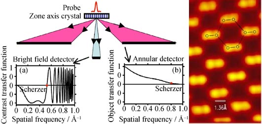
扫描透射电子显微镜(STEM)原子序数衬度像(Z-衬度像)具有分辨率高(可直接“观察”到晶体中原子的真实位置)、对化学组成敏感以及图像直观易解释等优点, 成为原子尺度研究材料微结构的强有力工具。本文介绍了STEM Z-衬度像成像原理、方法及技术特点, 并结合具体的高K栅介质材料 (如铪基金属氧化物、稀土金属氧化物和钙钛矿结构外延氧化物薄膜)对STEM在新一代高K栅介质材料研究中的应用进行了评述。 目前球差校正STEM Z-衬度的像空间分辨率已达亚埃级, 该技术在高K柵介质与半导体之间的界面微结构表征方面具有十分重要的应用。对此, 本文亦进行了介绍。
朱信华 , 李爱东 , 刘治国 . 扫描透射电子显微镜(STEM)在新一代高K栅介质材料的应用[J]. 无机材料学报, 2014 , 29(12) : 1233 -1240 . DOI: 10.15541/jim20140110
Scanning transmission electron microscopy (STEM) Z-contrast image has some advantages such as high image resolution (directly revealing the real positions of atoms in crystal), high compositional sensitivity and directly interpretable images, it becomes a powerful tool for investigating the microstructure of materials at atomic scale. In this review, the formation mechanisms, methods and features of the Z-contrast STEM images are introduced, and its applications in the new generation of high-k gate dielectrics (e.g., Hf-based metals oxides, rare-earth oxides and epitaxial perovskite oxides) are also reviewed. After aberration-correction the spatial resolution of the Z-contrast STEM images is as high as the sub-Å level, this technique is invaluable for characterizing the interfacial structures between high-K gate dielectrics and semiconductors. The related results are also introduced.
| [1] | LI D X.High-resolution transmission electron microscopy in materials science-developed history, current status and prospect. J. Chin. Electr. Microscopy Soc., 2000, 19(2): 81-83. |
| [2] | VARELA M, LUPINI A R, BENTHEM K V, et al.Materials characterization in the aberration-corrected scanning transmission electron microscope. Annu. Rev. Mater. Res., 2005, 35: 539-569. |
| [3] | WILK G D, WALLACE R M, ANTHONY J M.High-k gate dielectrics: current status and materials properties considerations. J. Appl. Phys., 2001, 89(10): 5243-5275. |
| [4] | ZHU X H, ZHU J M, LI A D, et al.Challenges in atomic-scale characterization of high-k dielectrics and metal gate electrodes for advanced CMOS gate stacks. J. Mater. Sci. Technol., 2009, 25(3): 289-313. |
| [5] | DELLBY N, KIRVANEK O L, NELLIST P D, et al.Progress in aberration-corrected scanning transmission electron microscopy. J. Electron Microscopy, 2001, 50(3): 177-185. |
| [6] | PENNUCOOK S J.Structure determination through Z-contrast microscopy. Advances in Imaging and Electron Physics, 2002, 123: 173-206. |
| [7] | PENNUCOOK S J, BOATNER L A.Chemically sensitive structure- imaging with a scanning transmission electron microscope. Nature, 1988, 336: 565-567. |
| [8] | BROWNING N D, WALLIS D J, NELLIST P D.EELS in the STEM: determination of materials properties on the atomic scale. Micron, 1997, 28(5): 333-348. |
| [9] | BROWNING N D, BUBAN J P, PROUTEAU C, et al.Investigating the atomic scale structure and chemistry of grain boundaries in High-Tc superconductors. Micron, 1999, 30(3): 425-436. |
| [10] | PENNUCOOK S J, JESSON D E.High-resolution Z-contrast imaging of crystals. Ultramicroscopy, 1991, 37(124):14-38. |
| [11] | PENNUCOOK S J, RAFFERTY B, NELLIST P D.Z-contrast imaging in and aberration-corrected scanning transmission electr on microscope. Microscopy and Microanalysis, 2000, 6: 343-352. |
| [12] | BUCHANAN D.Scaling the gate dielectric: materials, integration, and reliability. IBM J. Res. & Dev., 1999, 43(3): 245-264. |
| [13] | BERSUKER G, ZEITZOFF P, BROWN G, et al.Dielectrics for future transistors. Material Today, 2004, 7(1): 26-33. |
| [14] | ROBERSON J.High dielectric constant gate oxides for metal oxide Si transistors. Rep. Prog. Phys., 2006, 69(2): 327-396. |
| [15] | ZHU X H, ZHU J M, LIU Z G, et al.Characterization of high-K gate dielectrics by atomic-resolution electron microscopy: current progress and future prospects. J. Chin. Electr. Microscopy Soc.,2009, 28(3): 280-302. |
| [16] | GARFUNKELD E, GUSTAFSSON T, LYSAGHT P, et al.Structure, composition and order at interfaces of crystalline oxides and other high-K materials on silicon. FUTURE FAB Inter, 2006, 220: 349-360 |
| [17] | CRAVEN A J, MACKENZIE M, MCCOMB D W, et al. Investigating physical and chemical changes in high-K gate stacks using nanoanalytical electron microscopy. Microelectron Eng., 2005, 80: 90-97. |
| [18] | OSTEN H J, LAHA A, CZERNOHORSKY M, et al.Introducing crystalline rare-earth oxides into Si technologies. Phys. Stat. Sol.(a), 2008, 205(4): 695-707 . |
| [19] | LAHA A, FISSEL A, BUGIEL E, et al.Epitaxial multi-component rare earth oxide for high-K application. Thin Solid Films, 2007, 515(16): 6512-6517. |
| [20] | OSTEN H J, CZERNOHORSKY M, DARGIS R, et al.Integration of functional epitaxial oxides into silicon: from high-K application to nanostructures. Microelectron Eng., 2007, 84(9/10): 2222-2225. |
| [21] | BUSCH B W, PLUCHERY O, CHABAL Y J, et al.Materials characterization of alternative gate dielectrics. MRS Bull., 2002, 27(3): 206-211. |
| [22] | SCHLOM D G, HAENI J H.A thermodynamic approach to selecting alternative gate dielectrics. MRS Bull., 2002, 27(3): 198-204 . |
| [23] | MARCHIORI C, SOUSA M, GUILLER A, et al. Thermal stability of the SrTiO3/(Ba,Sr)O3 stacks epitaxially grown on Si. Appl. Phys. Lett., 2006, 88(7): 072913-1-3. |
| [24] | NORGA G J, MARCHIORI C, ROSSEL C, et al. Solid phase epitaxy of SrTiO3 on (Ba,Sr)O/Si(100): the relationship between oxygen stoichiometry and interface stability. J. Appl. Phys., 2006, 99(8): 84102-1-7. |
| [25] | KLENOV D O, SCHLOM D G, Li H, et al. The interface between single crystalline (001) LaAlO3 and (001) silicon. Jpn. J. Appl. Phys., 2005, 44(20-23): L617-L619. |
| [26] | AGUSTIN M P, FONSECA L R C, HOOKER J C, et al. Scanning transmission electron microscopy of gate stacks with HfO2 dielectrics and TiN electrodes. Appl. Phys. Lett., 2005, 87(12): 121909-1-3. |
| [27] | CHOI K, ALSHAREEF H N, WEN H C, et al. Effective work function modification of atomic-layer-deposited-TaN film by capping layer. Appl. Phys. Lett., 2006, 89(3): 032113-1-3. |
| [28] | ANDERSON S C, BIRKELAND C R, ANSTIS G R, et al.An approach to quantitative compositional profiling at near-atomic resolution using high-angle annular dark field imaging. Ultramicroscopy, 1997, 69(2): 83-103. |
| [29] | PENNUCOOK S J, JESSON D E, MCGIBBON A J, et al.High angle dark field STEM for advanced materials. J. Electron Microscopy, 1996, 45(1): 36-43. |
| [30] | BENTHEMA K V, LUPINI A R, KIM M Y, et al. Three-dimensional imaging of individual hafnium atoms inside a semiconductor device. Appl. Phys. Lett., 2005, 87(3): 034104-1-3. |
/
| 〈 |
|
〉 |