GaN单晶的HVPE生长与掺杂进展
齐占国1( ), 刘磊1, 王守志1(), 王国栋1, 俞娇仙2, 王忠新1, 段秀兰1, 徐现刚1, 张雷1()
), 刘磊1, 王守志1(), 王国栋1, 俞娇仙2, 王忠新1, 段秀兰1, 徐现刚1, 张雷1()
Progress in GaN Single Crystals: HVPE Growth and Doping
QI Zhanguo1(), LIU Lei1, WANG Shouzhi1(), WANG Guogong1, YU Jiaoxian2, WANG Zhongxin1, DUAN Xiulan1, XU Xiangang1, ZHANG Lei1()
), LIU Lei1, WANG Shouzhi1(), WANG Guogong1, YU Jiaoxian2, WANG Zhongxin1, DUAN Xiulan1, XU Xiangang1, ZHANG Lei1()
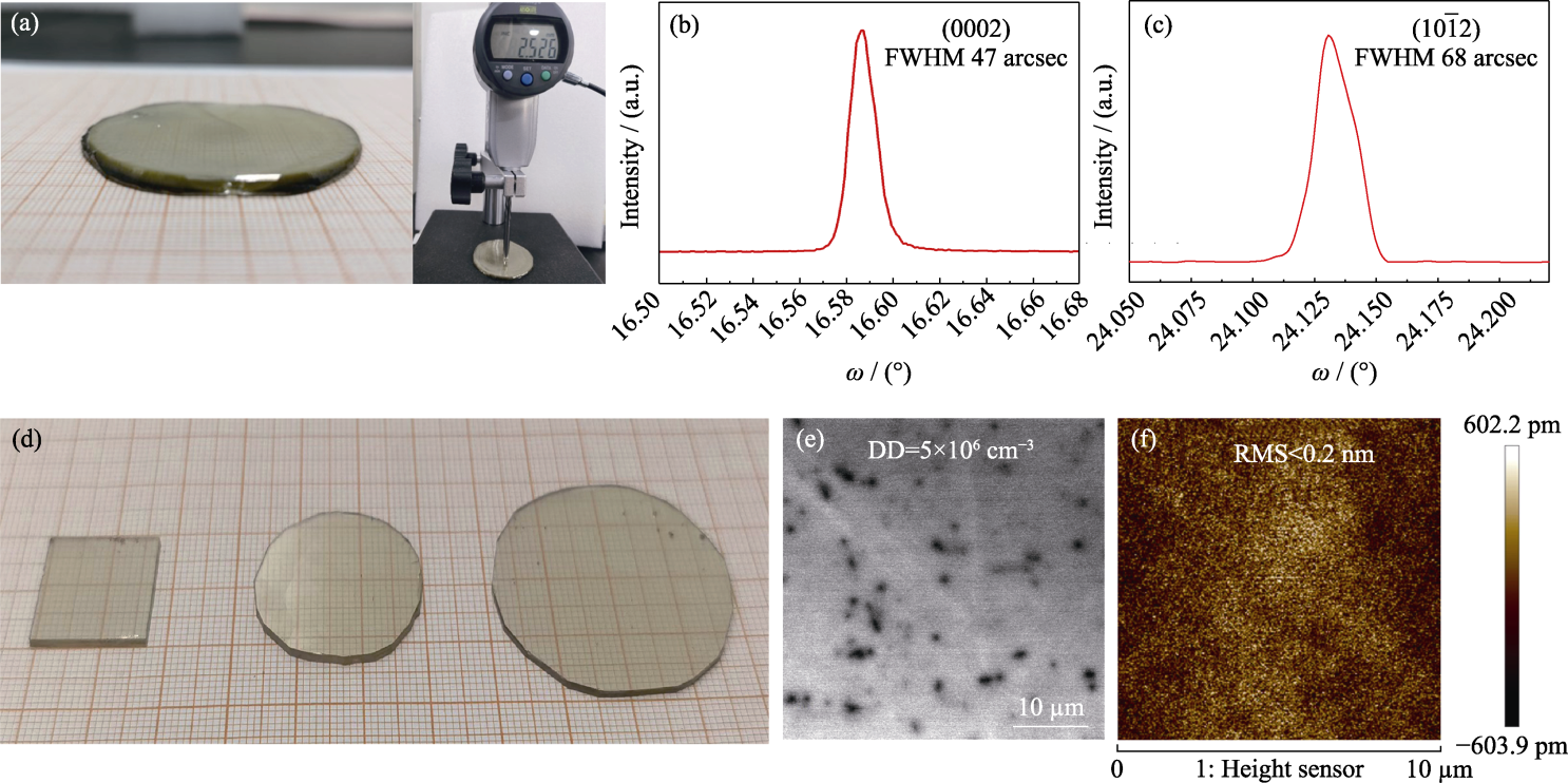
图3. HVPE生长的GaN晶体照片及质量表征
Fig. 3. Photos and characterization of GaN crystals grown by HVPE
(a) 2-inch 2.5 mm thick GaN crystal; (b) (0002) surface high-resolution XRD pattern; (c) (10¯12) high-resolution XRD pattern; (d) Image of GaN wafers; (e) CL image (dislocation density ~5×106 cm-2); (f) AFM image (RMS<0.2 nm in the range of 10 μm×10 μm)