GaN单晶的HVPE生长与掺杂进展
齐占国1( ), 刘磊1, 王守志1(), 王国栋1, 俞娇仙2, 王忠新1, 段秀兰1, 徐现刚1, 张雷1()
), 刘磊1, 王守志1(), 王国栋1, 俞娇仙2, 王忠新1, 段秀兰1, 徐现刚1, 张雷1()
Progress in GaN Single Crystals: HVPE Growth and Doping
QI Zhanguo1(), LIU Lei1, WANG Shouzhi1(), WANG Guogong1, YU Jiaoxian2, WANG Zhongxin1, DUAN Xiulan1, XU Xiangang1, ZHANG Lei1()
), LIU Lei1, WANG Shouzhi1(), WANG Guogong1, YU Jiaoxian2, WANG Zhongxin1, DUAN Xiulan1, XU Xiangang1, ZHANG Lei1()
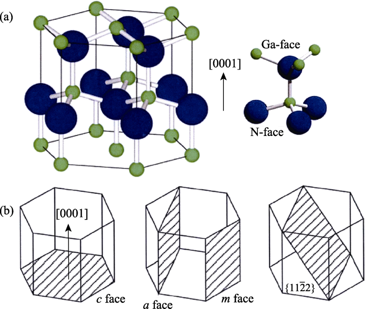
图1. GaN示意图[
Fig. 1. Schematic diagram of GaN[
(a) Hexagonal unit call (left) and the bond structure of GaN (right), with green balls indicating Ga atoms and blue balls indicating N atoms; (b) Polar face (left), non-polar face (middle) and one kind of semi-polar faces (right) of GaN crystal