新型GaN与ZnO衬底ScAlMgO4晶体的研究进展
张超逸1( ), 唐慧丽1(), 李宪珂1, 王庆国1, 罗平1, 吴锋1, 张晨波1, 薛艳艳1, 徐军1(), 韩建峰2, 逯占文2
), 唐慧丽1(), 李宪珂1, 王庆国1, 罗平1, 吴锋1, 张晨波1, 薛艳艳1, 徐军1(), 韩建峰2, 逯占文2
Research Progress of ScAlMgO4 Crystal: a Novel GaN and ZnO Substrate
ZHANG Chaoyi1(), TANG Huili1(), LI Xianke1, WANG Qingguo1, LUO Ping1, WU Feng1, ZHANG Chenbo1, XUE Yanyan1, XU Jun1(), HAN Jianfeng2, LU Zhanwen2
), TANG Huili1(), LI Xianke1, WANG Qingguo1, LUO Ping1, WU Feng1, ZHANG Chenbo1, XUE Yanyan1, XU Jun1(), HAN Jianfeng2, LU Zhanwen2
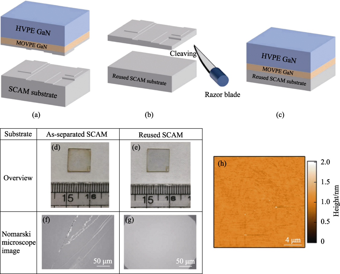
图11. SCAM衬底的再利用过程[
Fig. 11. SCAM substrate reuse process[
(a) GaN film is naturally separated from SCAM substrate during the growth and cooling process of HVPE; (b) Separated SCAM substrate being cleaved with a razor blade to prepare the reusable SCAM substrate; (c) GaN film grown by MOVPE and HVPE being performed on the reusable SCAM substrate; (d, f) Photo and Nomarski microscope image of naturally separated SCAM substrate; (e, g) Photo and Nomarski microscope image of SCAM substrate cleaved with a razor blade; (h) AFM image of SCAM substrate cleaved with a razor blade