PdSe2半导体薄膜的真空硒化法制备研究
王慧1,2( ), 张淑娟1,3, 陈亭伟1, 张传林1, 罗豪甦2, 郑仁奎1()
), 张淑娟1,3, 陈亭伟1, 张传林1, 罗豪甦2, 郑仁奎1()
Electronic Property of PdSe2 Thin Films Fabricated by Post-selenization of Pd Films
WANG Hui1,2(), ZHANG Shujuan1,3, CHEN Tingwei1, ZHANG Chuanlin1, LUO Haosu2, ZHENG Renkui1()
), ZHANG Shujuan1,3, CHEN Tingwei1, ZHANG Chuanlin1, LUO Haosu2, ZHENG Renkui1()
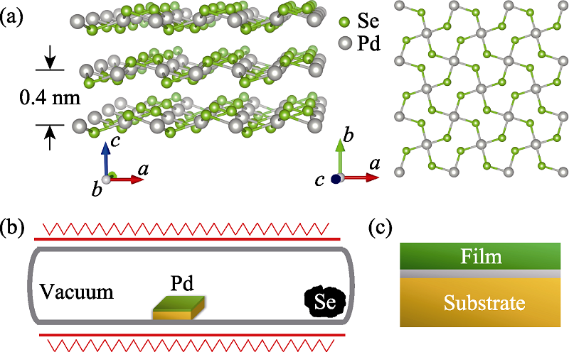
Fig. 1. Side and top view of the crystal structure of PdSe2 thin films (a), schematic illustration for the growth of PdSe2 films on SiO2/Si substrates by post-selenization of a Pd layer in an evacuated quartz ampule (b), and structure diagram of the PdSe2/SiO2/Si structure (c)
.