|
介质衬底上生长h-BN二维原子晶体的研究进展
|
|
张兴旺1,2,高孟磊1,2,孟军华1,2
|
|
Research Progress of Direct Growth of Two-dimensional Hexagonal Boron Nitride on Dielectric Substrates
|
ZHANG Xing-Wang 1,2,GAO Meng-Lei 1,2,MENG Jun-Hua 1,2
|
|
|
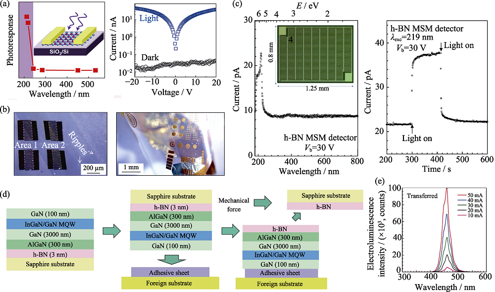
图6. (a)h-BN光探测器的响应光谱及其212 nm光照和暗态下的I-V曲线[60]; (b)转移下来的薄膜的光学显微镜图及其柔性器件的照片[61]; (c)偏压30 V下, h-BN MSM探测器的响应光谱和响应时间[62]; (d)量子阱器件的设计、释放和转移过程示意图[67]; (e)转移后器件的EL光谱[68]
|
Fig. 6. (a) Response spectrum of the h-BN detector and I-V curves under 212 nm laser irradiation and dark condition[60]; (b) Microscope image of the transferred film and the photograph of the flexible metal-semiconductormetal device[61]; (c) The relative spectral response and photocurrent decay kinetics of h-BN MSM detector measured at Vb = 30 V (Inset showing a microscope image of the h-BN MSM photodetector)[62]; (d) Schematic illustrations of the MQW materials design, release and transfer processes[67]; (e) Electroluminescence spectra from the transferred LED[68]
|
|
 |
|
|