介质衬底上生长h-BN二维原子晶体的研究进展
Research Progress of Direct Growth of Two-dimensional Hexagonal Boron Nitride on Dielectric Substrates
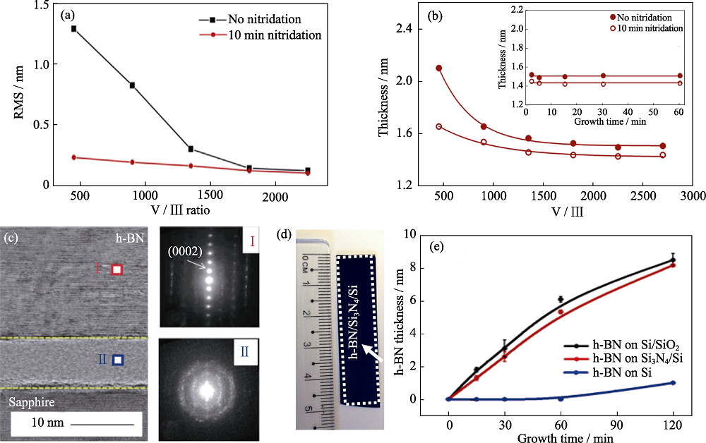
图5. (a)RMS随V/III比例变化的关系图; (b)不做表面氮处理与氮处理10 min条件下, BN厚度随V/III比例变化的关系图(插图是V/III比例为2250时, BN厚度随生长时间变化的关系图); (c)蓝宝石衬底上h-BN的截面STEM照片及对应区域的衍射图; (d)Si3N4/Si衬底上h-BN的照片; (e)Si3N4/Si, SiO2/Si和Si衬底上h-BN厚度与生长时间的关系图[
Fig. 5. (a) Plot of RMS determined by AFM vs. V/III; (b) Thickness vs. V/III for BN films grown on sapphire with and without the pre-growth nitridation process with insetshowing thickness vs. growth time for films grown using a V/III ratio of 2250; (c) Cross-sectional STEM image of h-BN grown on sapphire and diffraction patterns for selected areas I and II; (d) Camera view of h-BN on Si3N4/Si; (e) Variations of h-BN film thickness at different CVD growth times for Si3N4/Si, SiO2/Si, and Si substrates[