|
介质衬底上生长h-BN二维原子晶体的研究进展
|
|
张兴旺1,2,高孟磊1,2,孟军华1,2
|
|
Research Progress of Direct Growth of Two-dimensional Hexagonal Boron Nitride on Dielectric Substrates
|
ZHANG Xing-Wang 1,2,GAO Meng-Lei 1,2,MENG Jun-Hua 1,2
|
|
|
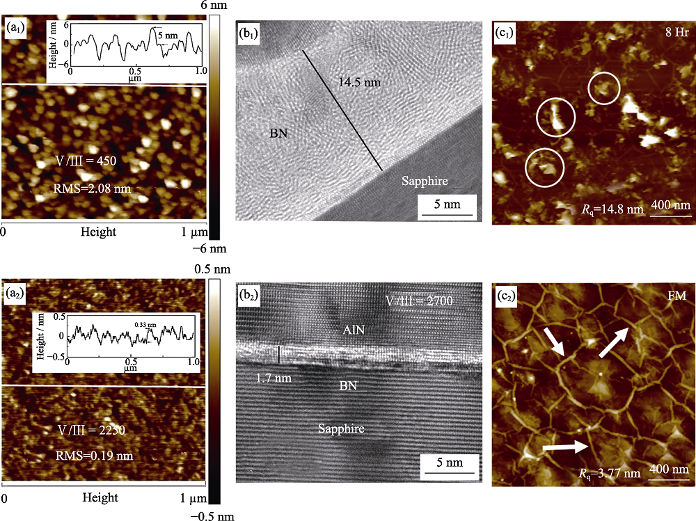
图2. (a)1000 ℃下生长30 min的BN薄膜的AFM形貌及粗糙度[35]: (a1)V/III = 450, (a2)V/III = 2250; (b)BN薄膜的截面TEM照片[35]: (b1)V/III = 450, (b2)V/III = 2700; (c)在(c1)流量连续和(c2)流量交替模式下, 生长8 h的h-BN薄膜的表面形貌[36,37]
|
Fig. 2. (a) AFM micrographs with line scans and surface roughness measured on BN films grown at 1000 ℃ for 30 min[35]: (a1) V/III = 450, (a2) V/III = 2250; (b) Cross sectional TEM images of BN layer deposited using (b1) V/III ratio of 450 and (b2) 2700[35]; (c) Surface topography of h-BN films deposited for 8 h (c1) under continuous flow conditions and (c2) using FM scheme[36,37]
|
|
 |
|
|