扫描透射电子显微镜(STEM)在新一代高K栅介质材料的应用
 , 李爱东
, 李爱东Applications of Scanning Transmission Electron Microscopy (STEM) in the New Generation of High-K Gate Dielectrics
ZHU Xin-Hua1 , LI Ai-Dong2 , LIU Zhi-Guo2
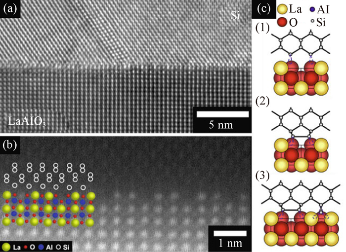
, LI Ai-DongFig. 9 a HRTEM and b HAADF-STEM images from an epitaxial SiLaAlO 3 interface showing an interface reconstruction where every third La column is missing at the interface. c Interface models based on the HAADF-STEM images [ 25 ]