陶瓷/石墨烯块体复合材料的研究进展
 , 陈彬彬
, 陈彬彬Recent Progress in Ceramic/Graphene Bulk Composites
LI Jian-Lin1 , CHEN Bin-Bin1 , ZHANG Wen1 , WANG Lian-Jun2 , JIANG Wan2
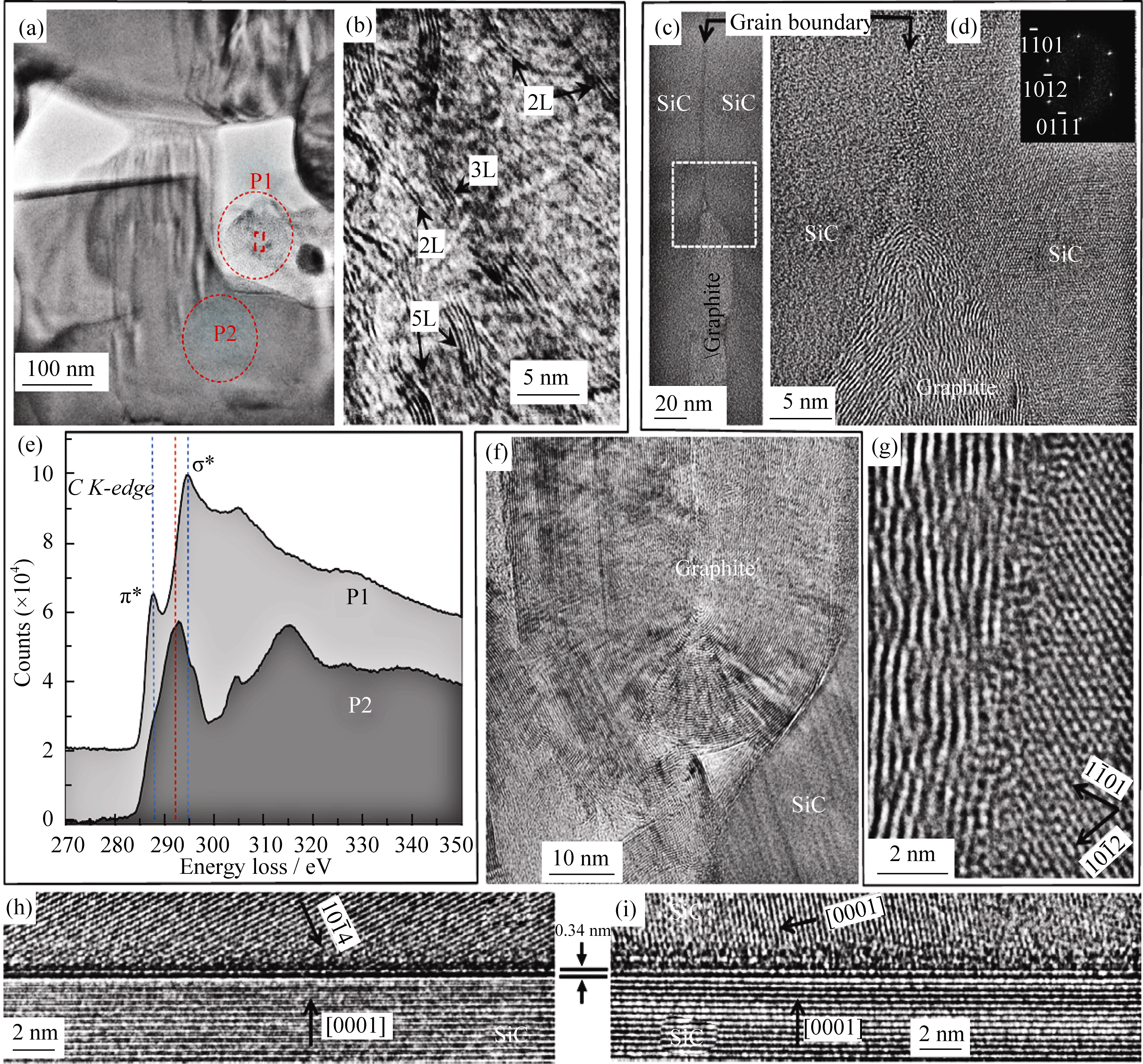
, CHEN Bin-BinFig. 15 TEM images of the #cod#x003b1;-SiC composite sample, showing several regions with different number of graphene layers. Region 1: a low magnification TEM image of the region of interest. b is a higher magnification image of the P1 region inside the highlighted rectangular region which is rich in sp 2 carbon, showing different cross-section views of few-layers graphene flakes 2L, 3L and 5L; the spacing between dark contrast lines is consistent with the spacing between graphene sheets. e are electron energy loss spectroscopy spectra after multiple-scattering background removal of the carbon K edge at positions P1 and P2, respectively. Region 2: c low magnification TEM image of a grain boundary with formation of a graphite island, d, g high-resolution TEM images of the same region, the inset is SEAD of the right side SiC grain. Region 3: f graphitic formation of several tens of nanometers. Region 4: h and i two different grain boundaries presenting bi-layer graphene [ 40 ]